TSMC to Expand Capacity for Mature and Specialty Nodes by 50%
TSMC this afternoon has disclosed that it will expand its production capacity for mature and specialized nodes by about 50% by 2025. The plan includes building numerous new fabs in Taiwan, Japan, and China. The move will further intensify competition between TSMC and such contract makers of chips as GlobalFoundries, UMC, and SMIC.
When we talk about silicon lithography here at AnandTech, we mostly cover leading-edge nodes used produce advanced CPUs, GPUs, and mobile SoCs, as these are devices that drive progress forward. But there are hundreds of device types that are made on mature or specialized process technologies that are used alongside those sophisticated processors, or power emerging smart devices that have a significant impact on our daily lives and have gained importance in the recent years. The demand for various computing and smart devices in the recent years has exploded by so much that this has provoked a global chip supply crisis, which in turn has impacted automotive, consumer electronics, PC, and numerous adjacent industries.
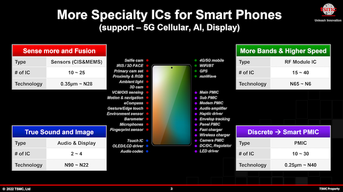
Modern smartphones, smart home appliances, and PCs already use dozens of chips and sensors, and the number (and complexity) of these chips is only increasing. These parts use more advanced specialty nodes, which is one of the reason why companies like TSMC will have to expand their production capacities of otherwise “old” nodes to meet growing demand in the coming years.
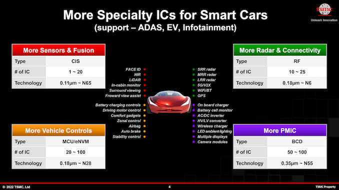
But there is another market that is about to explode: smart cars. Cars already use hundreds of chips, and semiconductor content is growing for vehicles. There are estimates that several years down the road the number of chips per car will be about 1,500 units – and someone will have to make them. Which is why TSMC rivals GlobalFoundries and SMIC have been increasing investments in new capacities in the last couple of years.
TSMC, which has among the largest CapEx budgets in the semiconductor industries (which is challenged only by Samsung) has in recent years been relatively quiet about their mature and specialty node production plans. But at their 2022 TSMC Technology Symposium, the company outlined its plans formally.
The company is investing in four new facilities for mature and specialty nodes:
- Fab 23 Phase 1 in Kumamoto, Japan. This semiconductor fabrication facility will make chips using TSMC’s N12, N16, N22, and N28 nodes and will have a production capacity of up to 45,000 300-mm wafer starts per month.
- Fab 14 Phase 8 in Tainan, Taiwan.
- Fab 22 Phase 2 in Kaohsiung, Taiwan.
- Fab 16 Phase 1B in Nanjing, China. TSMC currently makes chips on its N28 in China, though the new phase was once rumored to be capable of making chips using more advanced nodes.
Increasing mature/specialized capacity by 50% over the next three years is a big shift for the company, and one that will improve TSMC’s competitive positions on the market. What is perhaps more important is that the company’s specialty nodes are largely based on its common nodes, which allows at least some companies to re-use IP they once developed for compute or RF for a new application.
“[Our] specialty technology is quite unique as it is based on common technology platform [logic technology platform], so our unique strategy is to allow our customer to share or reuse many of the [common] IP,” said Kevin Zhang, senior vice president of business development at TSMC. “For example, you have RF capability, you build that RF on a common logic platform, but later you find ‘hey someone need a so-called ULV feature to support an IoT product application.’ You want to build that on a common platform so you can allow different product lines to be able to share IP across the board, this is very important for our customers so we do want to provide a integrated platform to address the market needs of customer from product perspective.’
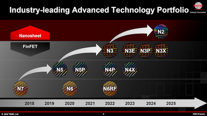
There are other advantages too. For example, TSMC’s N6RF allows chip designers to combine high-performance logic with RF, which enables them to build products such as modems and other, more unique solutions. Many companies are already familiar with TSMC’s N6 logic node, so now they have an opportunity to add RF connectivity to something that benefits from high performance. GlobalFoundries has a similar approach, but since the U.S.-based foundry does not have anything comparable to TSMC’s N6, TSMC has an indisputable advantage here.
With its common platform approach for mature nodes as well as specialized technologies, and 50% more capacity, TSMC will be able to offer the world more chips for smart and connected devices in the coming years. Furthermore, it will also benefit TSMC by significantly increasing the company’s revenues from mature and specialized nodes, as well as increasing pressure on their rivals.
Source: Recent News


