Marvell Announces First MoChi Architecture Modules: SoCs Go To Pieces
Much has been written over the last few years on the significant cost issues semiconductor companies are and will be facing over the coming years. While newer manufacturing nodes have increased transistor density and reduced power consumption, they have come at a cost of increased manufacturing and development costs for chips using these nodes. Yet more worrying for manufacturers, the costs of preparing chips for new nodes isn’t just rising but rising quickly, with mask sets already over a million dollars and expected to grow even further thanks to the high costs of developing masks for current multi-patterning technologies.
As a result semiconductor companies have been increasingly focused on containing costs, especially in the highly competitive and lower margin commodity markets, where customers are very sensitive to price and have many alternatives. These customers in turn still need higher performance parts to improve their own products, but they can’t necessarily afford to pay the full cost for a chip built on a cutting-edge node.
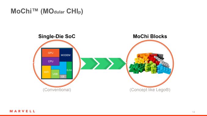
Looking to address this problem, earlier this year Marvell announced their Modular Chip (MoChi) architecture. The MoChi architecture in turn would attempt to control rising SoC costs by modularizing traditional SoCs and only manufacturing the most performance critical modules on a leading-edge node, while manufacturing the other modules on cheaper existing nodes. By splitting up a chip in this fashion, the number of transistors laid down on the leading-edge node would be held to a minimum, resulting in a smaller module that would be cheaper to design and cheaper to produce than a full SoC, all the while the other modules would be relatively cheap to produce and cheap to design (if not largely held over from existing designs to begin with).
After previously announcing the MoChi architecture and its design goals, this morning Marvell is announcing that the first two MoChi-enabled SoCs. The first of these is the AP806, a quad-core Cortex-A72 design that contains just the CPU, memory controller, and associated logic, and is designed for higher performance devices. Meanwhile at the other end of the spectrum is the ARMADA 3700, a more integrated MoChi module containing a dual-core Cortex-A53 processor setup along with additional networking IP and primarily designed for use in networking products.
Marvell is not disclosing what manufacturing node either module is being produced on, however in the case of the AP806 it is a likely bet that it is based on TSMC’s 16nm FinFET process given the focus on ARM’s high-performance Cortex-A72 processor. Meanwhile the ARMADA 3700 can be considered a toss-up; as MoChi is meant for post-28nm designs it’s possible it’s a 16nm design as well, though 20nm and 28nm are not out of the question if Marvell is focusing more on the customization possibilities of its modularity than die size and power efficiency.
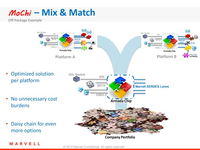
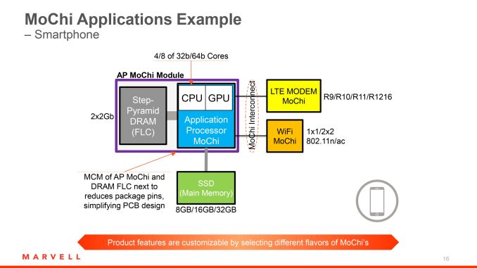
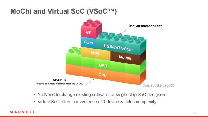
Meanwhile joining these two modules and completing the MoChi design will be other modules. Developed by both Marvell and third parties, Marvell has not announced any other modules at this time. However in discussing these modules, the company noted that they would contain secondary functions like I/O, security, WiFi, LTE, and other more traditional south bridge functionality. It’s by producing these modules on older processes (e.g. 28nm) that Marvell is able to contain costs, and meanwhile it gives them and customers the opportunity to mix and match modules to build an SoC with the specific functionality they’re after. And in the case of modules from third parties, this also serves as an avenue to integrate third party IP into what’s otherwise a Marvell SoC without Marvell having to go the semi-custom route of integrating multiple vendors’ IP into a single SoC.
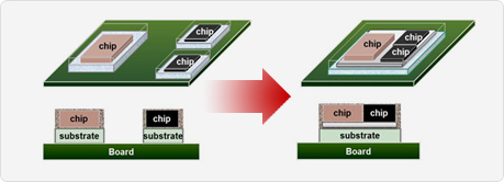
Getting back to MoChi itself, as these are the first modules based around the architecture, it’s interesting to note the tradeoffs that are involved in developing a MoChi SoC. While Marvell more immediately limits development costs and production costs via a smaller die on a leading-edge node, this is balanced with the fact that a MoChi chip is now a multi-chip module (MCM), which does have an impact on the development and power costs of connecting the modules, along with producing a larger package overall. So for Marvell there is a balancing act between driving down die costs without inflating other costs by too much.
Providing the actual interconnect functionality is a coherent, high-speed interconnect Marvell calls Aurora2, though it’s more frequently referred to as simply the MoChi interconnect. Based on cost and performance needs, the MoChi interconnect is available in what Marvell is calling both parallel and serial configurations. The parallel interconnect is faster, but is limited to short runs for cost and power reasons, whereas the serial interconnect is slower but cheaper as a result. For obvious reasons the parallel interconnect needs to run along a single SoC layer, whereas from Marvell’s comments it sounds like modules connected via the serial interconnect can be layered ala Package-on-Package technology.
Meanwhile thanks to the MoChi interconnect, Marvell is able to hide from software the fact that MoChi spreads out the different functions of an SoC over multiple modules. As a result the use of multiple modules is transparent to software, which continues to see the SoC as a single monolithic SoC. Marvell calls this a Virtual SoC design.
Unfortunately Marvell is not disclosing much in the way of details on the manufacturing side of matters, however from what we know about TSMC’s catalog we can take an educated guess at what Marvell is doing. Most likely the company is using TSMC’s Chip-On-Wafer-On-Substrate service (CoWoS), which as implied by the name involves building multiple dies on a single shared substrate. CoWoS is designed in part for precisely the kind of mixed-process modules that Marvell’s MoChi architecture uses, with the single shared substrate allowing for shorter runs of higher density connections. This in turn would allow Marvell to keep interconnect power in check, something that’s especially important for the MoChi parallel interconnect.
The tradeoff for Marvell here is that the shared substrate itself drives up costs and the use of Through-Silicon-Vias – which we first saw with HBM – also presents cost challenges. Which given this, it’s likely that CoWoS is only being used for the parallel interconnect, especially given the cost goals of the slower serial interconnect.
Wrapping things up, in discussing today’s announcement Marvell also confirmed that the announcement of the AP806 and ARMADA 3700 closely follows the sampling of these two modules. The company received their first samples in the lab for a few weeks now, so ideally customer samples shouldn’t be too far behind. At this point Marvell expects that MoChi chips should start showing up in products by the end of next year.
As for what products they’ll appear in, that’s ultimately up to what customers want. But given the fact that MoChi is a cost control technology, it stands to reason that it’s more likely to show up in cost-sensitive embedded applications than high-profile mobile devices. Marvell for their part notes that a lot of the initial focus is on enterprise and data center networking – particularly with the networking-optimized ARMADA 3700 – and along with storage products these are likely the first markets that we’ll see MoChi-based SoCs show up in.

