Wearables


LG Announces the G Watch R

LG Announces the G Watch R

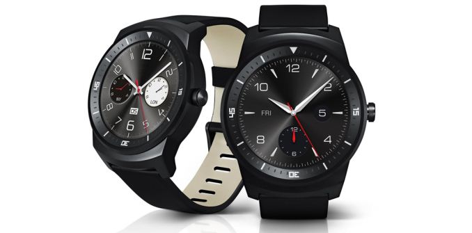
It looks like LG really isn’t keen on waiting for IFA to reveal some of its new products. Yesterday we detailed the announcement of the LG G3 Stylus, and today LG is giving a sneak peak at its first smartwatch with a round face. It’s called the LG G Watch R, and as you may have guessed, the R stands for round. 

At its core, the G Watch R is basically the same device as the original G Watch. It uses Qualcomm’s APQ8026 quad Cortex-A7 part running at 1.2GHz, paired with an Adreno 305 and 512MB of RAM plus 4GB of NAND. It also retains the G Watch’s IP67 rating for submersion in water up to 1 meter deep for 30 minutes. The battery receives a small 10mAh bump from 400mAh to 410mAh. A heart rate monitor has been added, taking away one of Samsung’s points of differentiation with their Gear Live smartwatch.

The real changes come with the display and the build. The original G Watch has a square display. The G Watch R sports a 1.3″ plastic OLED (P-OLED) display with a 320×320 resolution (which likely means the vertical and horizontal resolution at the watch’s widest points in those directions) that takes up 100% of the watch face. This contrasts with the yet to be released Moto 360 which has a 1.5″ rounded display but has a segment at the bottom which isn’t part of the usable display area. The display is surrounded by a stainless steel bezel and frame, and comes with a leather strap.

The G Watch R is the first smartwatch I’ve seen that really looks like a traditional analog watch. The Moto 360 is definitely up there with it, but for me the gap in the display on the Moto 360 takes away from it significantly.

LG says that the G Watch R will be available in Q4 of this year. There’s no word on pricing but it’ll likely be higher than the standard G Watch which currently sells for $229. More details about the G Watch R will be revealed soon at IFA Berlin.

Source: LG via Android Police

Intel Announces XMM6255: The World's Smallest Standalone 3G Modem

Intel Announces XMM6255: The World’s Smallest Standalone 3G Modem

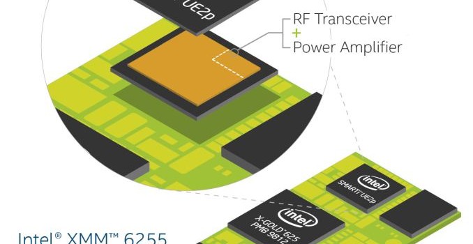
Today Intel announced their XMM6255 modem which is aimed at providing 3G network connectivity to the many future connected devices that will make up the Internet of Things (IoT). At approximately 300mm^2 in size, Intel is claiming that XMM6255 is the world’s smallest standalone 3G modem. Their hope is that its small size will allow it to be integrated into small internet connected devices such as wearables, small appliances, and security devices. 

XMM6255 uses Intel’s X-GOLD 625 baseband and its SMARTI UE2p transceiver which is the first transceiver that integrates the transmit and receive functionality and the 3G power amplifier on a single die with its own power management. Intel claims this protects the modem from damage caused by excessive heat, voltage spikes, or overcurrent, which makes it a good choice for IoT applications like safety monitors and sensors where a hardware failure could present a safety risk. Integrating the power amplifier and transceiver on a single chip also reduces the bill of materials and power consumption, which allows XMM6255 to be put in low-cost and low-power devices.

XMM6255 typically comes in a dual-band HSPA configuration with 7.2Mbps downstream and 5.76Mbps upstream speeds. Up to quad-band 2G support can be optionally added, but requires an external power amplifier that Intel is billing as low-cost. A-GPS is also supported but is again optional.

XMM6255 represents another move by Intel to becoming a big part of the IoT market. Intel expects that the IoT market will be made up of billions of devices in the coming years, and getting a head start is a good way to make sure that many of them have Intel inside.

ARM's Cortex M: Even Smaller and Lower Power CPU Cores

ARM’s Cortex M: Even Smaller and Lower Power CPU Cores

ARM (and its partners) were arguably one of the major causes of the present day smartphone revolution. While AMD and Intel focused on using Moore’s Law to drive higher and higher performing CPUs, ARM and its partners used the same physics to drive integration and lower power. The result was ultimately the ARM11 and Cortex A-series CPU cores that began the revolution and continue to power many smartphones today. With hopes of history repeating itself, ARM is just as focused on building an even smaller, even lower power family of CPU cores under the Cortex M brand.

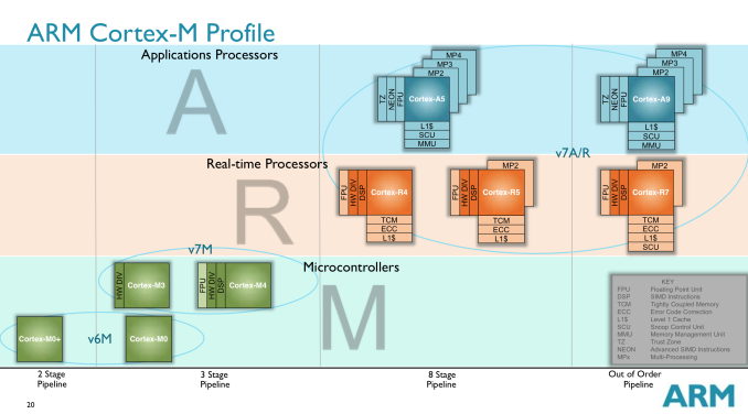
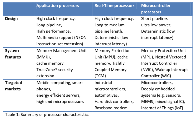
We’ve talked about ARM’s three major families of CPU cores before: Cortex A (applications processors), Cortex R (real-time processors) and Cortex M (embedded/microcontrollers). Although Cortex A is what we mostly talk about, Cortex M is becoming increasingly important as compute is added to more types of devices.
Wearables are an obvious fit for Cortex M, yet the initial launch of Android Wear devices bucked the trend and implemented Cortex A based SoCs. A big part of that is likely due to the fact that the initial market for an Android Wear device is limited, and thus a custom designed SoC is tough to justify from a financial standpoint (not to mention the hardware requirements of running Android outpace what a Cortex M can offer). Looking a bit earlier in wearable history and you’ll find a good number of Cortex M based designs including the FitBit Force and the Pebble Steel. I figured it’s time to put the Cortex M’s architecture, performance and die area in perspective.

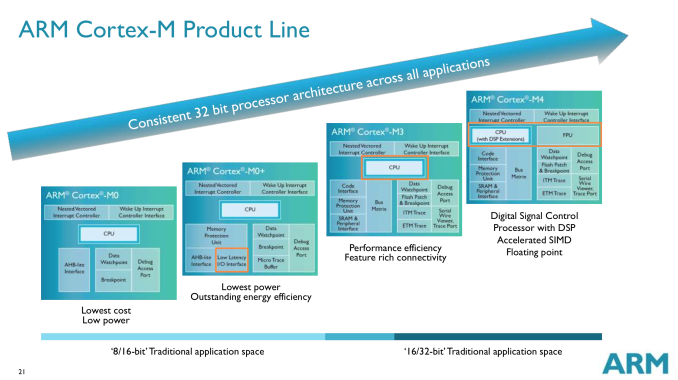
We’re very much in the early days of the evolution of Cortex M. The family itself has five very small members: M0, M0+, M1, M3 and M4. For the purposes of this article we’ll be focusing on everything but Cortex M1. The M1 is quite similar to the M0 but focuses more on FPGA designs.

Before we get too far down the architecture rabbit hole it’s important to provide some perspective. At a tech day earlier this year, ARM presented this data showing Cortex M die area:
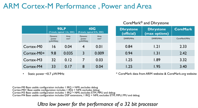
By comparison, a 40nm Cortex A9 core would be roughly around 2.5mm^2 range or a single core. ARM originally claimed the Cortex A7 would be around 1/3 – 1/2 of the area of a Cortex A8, and the Cortex A9 is roughly equivalent to the Cortex A8 in terms of die area, putting a Cortex A7 at 0.83mm^2 – 1.25mm^2. In any case, with Cortex M we’re talking about an order of magnitude smaller CPU core sizes.

The Cortex M0 in particular is small enough that SoC designers may end up sprinkling in multiple M0 cores in case they need the functionality later on. With the Cortex M0+ we’re talking about less than a hundredth of a square millimeter in die area, even the tightest budgets can afford a few of these cores.

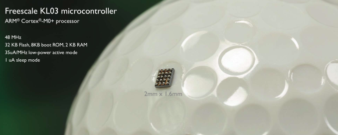
In fact, entire SoCs based on Cortex M CPU cores can be the size of a single Cortex A core. ARM provided this shot of a Freescale Cortex M0+ design in the dimple of a golf ball:
ARM wouldn’t provide me with comparative power metrics for Cortex M vs. Cortex A series parts, but we do have a general idea about performance:

Estimated Core Performance
  ARM Cortex M0/M0+ ARM Cortex M3/M4 ARM11 ARM Cortex A7 ARM Cortex A9 Qualcomm Krait 200
DMIPS/MHz 0.84/0.94 1.25 1.25 1.9 2.5 3.3

In terms of DMIPS/MHz, Cortex M parts can actually approach some pretty decent numbers. A Cortex M4 can offer similar DMIPS/MHz to an ARM11 (an admittedly poor indicator of overall performance). The real performance differences come into play when you look at shipping frequencies, as well as the type of memory interface built around the CPU. Cortex M designs tend to be largely SRAM and NAND based, with no actual DRAM. You’ll note that the M3/M4 per clock performance is identical, that’s because the bulk of what the M4 adds is in the form of other hardware instructions not measured by Dhrystone performance.

Instruction set compatibility varies depending on the Cortex M model we’re talking about. The M0 and M0+ both implement ARM’s v6-M instruction profile, while the M3 and M4 support ARM’s v7-M. As you go up the family in terms of performance you get access to more instructions (M3 adds hardware divide, M4 adds DSP and FP instructions):
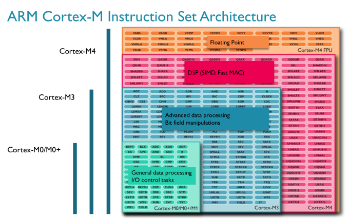
Each Cortex M chip offers a superset of the previous model’s instructions. So a Cortex M3 should theoretically be able to execute code for a Cortex M0+ (but not necessarily vice versa).

You also get support for more interrupts the higher up you go on the Cortex M ladder. The Cortex M0/M0+ designs support up to 32 interrupts, but if you move up to the M3/M4 you get up to 240.

All Cortex M processors have 32-bit memory addressability and the exact same memory map across all designs. ARM’s goal with these chips is to make moving up between designs as painless as possible.

While we’ve spent the past few years moving to out-of-order designs in smartphone CPUs, the entire Cortex M family is made up of very simple, in-order architectures. The pipelines themselves are similarly simplified:
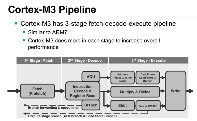
Cortex M0, M3 and M4 all feature 3-stage in-order pipelines, while the M0+ shaves off a stage of the design. In the 3-stage designs there’s an instruction fetch, instruction decode and a single instruction execute stage. In the event the decoder encounters a branch instruction, there’s a speculative instruction fetch that grabs the instruction at the branch target. This way regardless of whether or not the branch is taken, the next instruction is waiting with at most a 1 cycle delay.

These aren’t superscalar designs, there’s only a 1-wide path for instruction flow down the pipeline and not many execution units to exploit. The Cortex M3 and M4 add some more sophisticated units (hardware integer divide in M3, MAC and limited SIMD in M4), but by and large these are simple cores for simple needs.

The range of operating frequencies for these cores is relatively low. ARM typically expects to see Cortex M designs in the 20 – 150MHz range, but the cores are capable of scaling as high as 800MHz (or more) depending on process node. There’s a corresponding increase in power consumption as well, which is why we normally see lower clocked Cortex M designs.
Similar to the Cortex A and R lines, the Cortex M family has a roadmap ahead of it. ARM recently announced a new CPU design center in Taiwan, where Cortex M based cores will be designed. I view the Cortex M line today quite similarly to the early days of the Cortex A family. There’s likely room for a higher performing option in between Cortex M4 and Cortex A7. If/when we get such a thing I feel like we may see the CPU building block necessary for higher performance wearable computing.