Storage


Sharkoon Launches Rapid-Case USB 3.1 Type-C Storage Device DIY Kit

Sharkoon Launches Rapid-Case USB 3.1 Type-C Storage Device DIY Kit

Sharkoon has introduced a DIY kit that lets users build their own external storage devices with the USB 3.1 Type-C interface. The kit is not expensive and resembles similar devices from other makers: it contains an enclosure for a drive as well as a USB 3.1 Type-C cable. The key element here is Type-C, although as with many devices of a similar nature, the 10 Gbps is limited by the chipset to 8 Gbps, and then further by the SATA protocol.

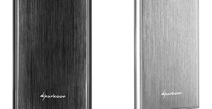
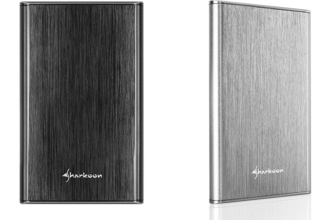
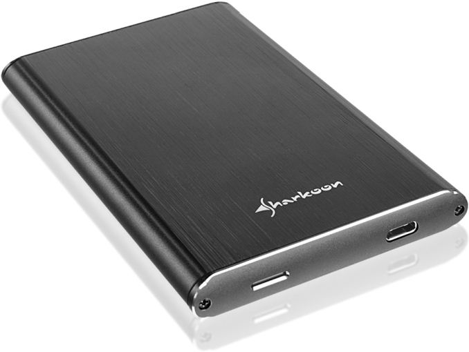
The Sharkoon Rapid-Case 2.5” USB 3.1 Type-C is a sleek enclosure (132×80×14 mm) made of black or silver brushed aluminum that can house a 2.5”/9.5 mm storage device and has a USB 3.1 Type-C header. The chassis weighs 83 grams and when populated with an HDD, its weight will increase to something like 170 ~ 230 grams depending on the drive used. The only thing that owners need to do to use the device is to install an appropriate pre-formatted HDD or SSD inside. 

The chassis contains ASMedia’s ASM1142 PCIe-to-USB 3.1 Gen 2 bridge as well as ASMedia’s ASM1351 USB-to-SATA bridge. The ASM1142 is a PCIe 3.0 x1 chip supporting a maximum bandwidth of up to 8 Gbps, which is below 10 Gbps specified by the USB 3.1 Gen 2 standard, but since this chip is used on loads of USB 3.1 Gen 2-supporting motherboards, this is not really a limitation for the Sharkoon Rapid-Case. Meanwhile, the USB-to-SATA bridge not only downs physical bandwidth to 6 Gbps, but it further reduces it by the overhead introduced by SATAS’s 8b/10b encoding. In the end, even if the Sharkoon Rapid-Case is populated by a high-end SSD, performance of the latter will be limited by SATA, not USB 3.1 Gen 2. In fact, this is the case with a lot of USB 3.1 Type-C storage devices: while they formally support 10 Gbps data rate, they use SATA drives inside with a maximum throughput of 6 Gbps (which is still higher than what you get from USB 3.0-supporting devices at 5 Gbps).

Despite the fact that right now not a lot of external storage devices (factory-made or DIY) can take advantage of USB 3.1 Gen 2’s 10 Gbps data rate, it is important that such devices make it to the market in general. Nowadays many new PCs feature USB Type-C ports and it is important to build up an ecosystem of devices with this interface. Furthermore, if you need a lot of storage space, you are going to use a 2.5″ HDD that has a maximum media to host transfer rate of less than ~200 MB/s and thus not requiring even 5 Gbps of USB 3.0.

The Sharkoon Rapid-Case 2.5″ USB 3.1 Type-C is available from select retailers in Europe for the suggested retail price of €24.99.

Related Reading:

Sharkoon Launches Rapid-Case USB 3.1 Type-C Storage Device DIY Kit

Sharkoon Launches Rapid-Case USB 3.1 Type-C Storage Device DIY Kit

Sharkoon has introduced a DIY kit that lets users build their own external storage devices with the USB 3.1 Type-C interface. The kit is not expensive and resembles similar devices from other makers: it contains an enclosure for a drive as well as a USB 3.1 Type-C cable. The key element here is Type-C, although as with many devices of a similar nature, the 10 Gbps is limited by the chipset to 8 Gbps, and then further by the SATA protocol.

The Sharkoon Rapid-Case 2.5” USB 3.1 Type-C is a sleek enclosure (132×80×14 mm) made of black or silver brushed aluminum that can house a 2.5”/9.5 mm storage device and has a USB 3.1 Type-C header. The chassis weighs 83 grams and when populated with an HDD, its weight will increase to something like 170 ~ 230 grams depending on the drive used. The only thing that owners need to do to use the device is to install an appropriate pre-formatted HDD or SSD inside. 

The chassis contains ASMedia’s ASM1142 PCIe-to-USB 3.1 Gen 2 bridge as well as ASMedia’s ASM1351 USB-to-SATA bridge. The ASM1142 is a PCIe 3.0 x1 chip supporting a maximum bandwidth of up to 8 Gbps, which is below 10 Gbps specified by the USB 3.1 Gen 2 standard, but since this chip is used on loads of USB 3.1 Gen 2-supporting motherboards, this is not really a limitation for the Sharkoon Rapid-Case. Meanwhile, the USB-to-SATA bridge not only downs physical bandwidth to 6 Gbps, but it further reduces it by the overhead introduced by SATAS’s 8b/10b encoding. In the end, even if the Sharkoon Rapid-Case is populated by a high-end SSD, performance of the latter will be limited by SATA, not USB 3.1 Gen 2. In fact, this is the case with a lot of USB 3.1 Type-C storage devices: while they formally support 10 Gbps data rate, they use SATA drives inside with a maximum throughput of 6 Gbps (which is still higher than what you get from USB 3.0-supporting devices at 5 Gbps).

Despite the fact that right now not a lot of external storage devices (factory-made or DIY) can take advantage of USB 3.1 Gen 2’s 10 Gbps data rate, it is important that such devices make it to the market in general. Nowadays many new PCs feature USB Type-C ports and it is important to build up an ecosystem of devices with this interface. Furthermore, if you need a lot of storage space, you are going to use a 2.5″ HDD that has a maximum media to host transfer rate of less than ~200 MB/s and thus not requiring even 5 Gbps of USB 3.0.

The Sharkoon Rapid-Case 2.5″ USB 3.1 Type-C is available from select retailers in Europe for the suggested retail price of €24.99.

Related Reading:

Adesto EcoXiP: Optimizing Memory Interfaces For Embedded Systems

Adesto EcoXiP: Optimizing Memory Interfaces For Embedded Systems

There is no Moore’s Law for flash memory. Unlike transistors, flash memory cells can no longer be made any smaller or faster without incurring reliability tradeoffs that negate the benefits of a process shrink. This has forced the solid state storage industry to look elsewhere for potential improvements. The long-term hopes are focused on a variety of non-volatile memory technologies that are years away from reaching the cost and density of NAND flash, but promise vast improvements to endurance, latency or power consumption. In the meantime, the challenge is to reduce cost or increase the performance that is possible from flash memory by changing how it is organized and accessed.

In the PC SSD market, two major shifts are underway to satisfy the need for continued progress in spite of the stagnation of the fundamental underlying memory cell technology. 3D NAND flash is replacing planar NAND flash, enabling density to continue growing and cost per bit to decline further while keeping the memory cell large enough to provide acceptable write endurance. Further up the storage stack, PCIe and the NVMe protocol allow for substantial improvements in throughput and latency as compared with the SATA interface.

But the SSD market is hardly the only outlet for flash memory technology. 3D NAND flash is beginning to replace planar NAND in smartphones and memory cards, and faster host interfaces are available for those markets. For even smaller embedded systems, NOR flash is still used. In these markets, low power and cost are often a higher priority than capacity and performance. The increasing popularity of the Internet of Things means many of those devices now have to include full network stacks supporting IPv6 and LTE, and thus their storage requirements have increased substantially.

Adesto is one of the many companies developing a new non-volatile memory, but their conductive bridging RRAM (CBRAM) so far only offers sub-megabit capacities. Adesto’s flash memory products are tailored for low-power embedded and IoT applications. Optimizing a memory product for these uses typically means using a low pin count interface like SPI and implementing extremely low-power sleep states. Erase block sizes are tuned to suit expected access patterns.

Adesto’s latest family of flash memory products makes some more drastic changes. Their EcoXiP line is intended for systems with an Execute In Place (XiP) memory architecture where the processor fetches code directly from flash into the instruction cache rather than loading it into a separate DRAM or SRAM bank. XiP systems save money by requiring less RAM, but at the cost of making CPU performance highly dependent on the performance of the flash.

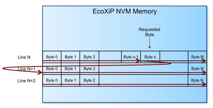
EcoXiP introduces a new mode for reading data that is designed to minimize the latency and command overhead of handling instruction cache misses. When the processor needs to branch to an address that is not in the instruction cache, it can issue a read request starting at the exact byte that is required. After the unavoidable latency of issuing the command and waiting for the flash to be read, the EcoXiP memory begins streaming the data from the requested byte. After reaching the end of the cache line the EcoXiP memory automatically wraps around to the earlier portion of the cache line so that the processor can fully populate that cache line while execution continues. The EcoXiP memory can then optionally proceed to sequentially stream subsequent cache lines in-order without requiring new read commands and addresses to be issued. Adesto estimates that the combination of delivering the most important byte first and enabling fast pre-fetching can increase effective CPU performance by over 40% for the case of a 266MHz processor using a 133MHz Octal SPI interface to flash with 100ns access time.

EcoXiP memory devices also support configuring the memory to behave as two independent banks. A single NOR flash bank cannot perform reads and writes simultaneously, which for an XiP device typically means the flash has to be treated as effectively a ROM device. Partitioning the device into separate banks allows the same chip to be used for both XiP operation and data logging, or to allow a software update to be installed to the second bank without suspending execution from the first bank.

The obvious downside to these innovations is that it is non-standard behavior. SPI itself is not a formal standard, but it is a widely supported de facto standard that has been around for decades, and JEDEC has defined a standard for querying the capabilities of SPI flash devices (similar to SPD and XMP for DRAM modules). Adesto’s protocol extensions require modifications to the processor’s memory controller and using EcoXiP will influence other system-level design decisions about memory and storage. Adesto has secured the support of microcontroller vendor NXP and IP vendors Synopsys and Mobiveil, so they should have no trouble building the market of devices that support EcoXiP memory.

Just as NVMe’s benefits over SATA will continue to help as SSDs using new persistent memories like 3D XPoint instead of flash come to market, Adesto’s protocol optimizations are not limited to just flash memory devices. Since most new persistent memory technologies will initially be available in capacities too small to directly replace NAND flash for SSD use and many of those technologies will be more economical to use as discrete memory devices rather than embedded memory integrated on SoCs, we will probably see several vendors producing specialized memory devices with optimizations similar to those used in Adesto’s EcoXiP.

EcoXiP memory is initially available as a 32Mb (4MB) device rated for 100,000 Program/Erase cycles and 20 year data retention, with a maximum transfer rate of 266MB/s. Capacities up to 128Mb (16MB) are planned.

Adesto EcoXiP: Optimizing Memory Interfaces For Embedded Systems

Adesto EcoXiP: Optimizing Memory Interfaces For Embedded Systems

There is no Moore’s Law for flash memory. Unlike transistors, flash memory cells can no longer be made any smaller or faster without incurring reliability tradeoffs that negate the benefits of a process shrink. This has forced the solid state storage industry to look elsewhere for potential improvements. The long-term hopes are focused on a variety of non-volatile memory technologies that are years away from reaching the cost and density of NAND flash, but promise vast improvements to endurance, latency or power consumption. In the meantime, the challenge is to reduce cost or increase the performance that is possible from flash memory by changing how it is organized and accessed.

In the PC SSD market, two major shifts are underway to satisfy the need for continued progress in spite of the stagnation of the fundamental underlying memory cell technology. 3D NAND flash is replacing planar NAND flash, enabling density to continue growing and cost per bit to decline further while keeping the memory cell large enough to provide acceptable write endurance. Further up the storage stack, PCIe and the NVMe protocol allow for substantial improvements in throughput and latency as compared with the SATA interface.

But the SSD market is hardly the only outlet for flash memory technology. 3D NAND flash is beginning to replace planar NAND in smartphones and memory cards, and faster host interfaces are available for those markets. For even smaller embedded systems, NOR flash is still used. In these markets, low power and cost are often a higher priority than capacity and performance. The increasing popularity of the Internet of Things means many of those devices now have to include full network stacks supporting IPv6 and LTE, and thus their storage requirements have increased substantially.

Adesto is one of the many companies developing a new non-volatile memory, but their conductive bridging RRAM (CBRAM) so far only offers sub-megabit capacities. Adesto’s flash memory products are tailored for low-power embedded and IoT applications. Optimizing a memory product for these uses typically means using a low pin count interface like SPI and implementing extremely low-power sleep states. Erase block sizes are tuned to suit expected access patterns.

Adesto’s latest family of flash memory products makes some more drastic changes. Their EcoXiP line is intended for systems with an Execute In Place (XiP) memory architecture where the processor fetches code directly from flash into the instruction cache rather than loading it into a separate DRAM or SRAM bank. XiP systems save money by requiring less RAM, but at the cost of making CPU performance highly dependent on the performance of the flash.

EcoXiP introduces a new mode for reading data that is designed to minimize the latency and command overhead of handling instruction cache misses. When the processor needs to branch to an address that is not in the instruction cache, it can issue a read request starting at the exact byte that is required. After the unavoidable latency of issuing the command and waiting for the flash to be read, the EcoXiP memory begins streaming the data from the requested byte. After reaching the end of the cache line the EcoXiP memory automatically wraps around to the earlier portion of the cache line so that the processor can fully populate that cache line while execution continues. The EcoXiP memory can then optionally proceed to sequentially stream subsequent cache lines in-order without requiring new read commands and addresses to be issued. Adesto estimates that the combination of delivering the most important byte first and enabling fast pre-fetching can increase effective CPU performance by over 40% for the case of a 266MHz processor using a 133MHz Octal SPI interface to flash with 100ns access time.

EcoXiP memory devices also support configuring the memory to behave as two independent banks. A single NOR flash bank cannot perform reads and writes simultaneously, which for an XiP device typically means the flash has to be treated as effectively a ROM device. Partitioning the device into separate banks allows the same chip to be used for both XiP operation and data logging, or to allow a software update to be installed to the second bank without suspending execution from the first bank.

The obvious downside to these innovations is that it is non-standard behavior. SPI itself is not a formal standard, but it is a widely supported de facto standard that has been around for decades, and JEDEC has defined a standard for querying the capabilities of SPI flash devices (similar to SPD and XMP for DRAM modules). Adesto’s protocol extensions require modifications to the processor’s memory controller and using EcoXiP will influence other system-level design decisions about memory and storage. Adesto has secured the support of microcontroller vendor NXP and IP vendors Synopsys and Mobiveil, so they should have no trouble building the market of devices that support EcoXiP memory.

Just as NVMe’s benefits over SATA will continue to help as SSDs using new persistent memories like 3D XPoint instead of flash come to market, Adesto’s protocol optimizations are not limited to just flash memory devices. Since most new persistent memory technologies will initially be available in capacities too small to directly replace NAND flash for SSD use and many of those technologies will be more economical to use as discrete memory devices rather than embedded memory integrated on SoCs, we will probably see several vendors producing specialized memory devices with optimizations similar to those used in Adesto’s EcoXiP.

EcoXiP memory is initially available as a 32Mb (4MB) device rated for 100,000 Program/Erase cycles and 20 year data retention, with a maximum transfer rate of 266MB/s. Capacities up to 128Mb (16MB) are planned.

G-Technology G-DRIVE slim SSD USB-C 500GB External SSD Capsule Review

G-Technology G-DRIVE slim SSD USB-C 500GB External SSD Capsule Review

Flash-based external direct-attached storage (DAS) devices have been rapidly evolving over the last few years. The emergence of USB 3.1 Gen 2 Type-C has led to external peripherals adopting it for the host interface. DAS units are no exception, and we have seen vendors release a number of Type-C devices over the last year or so. On the storage media side, there has been a move towards cheaper flash, with TLC as the primary driver. High-performance flash-based DAS units carry a premium as they are still reliant on MLC flash for providing consistent performance.

In the last five years, Western Digital (WD) has made a string of acquisitions as part of the overall consolidation trend in the market. The two key ones have been HGST and SanDisk. Along with HGST, WD also acquired the G-Technology brand. This brand has been catering to the storage demands of content creators for multimedia acquisition, editing and distribution. Their products range from bus-powered rugged portable hard drives and SSDs to rackmount enclosures for multiple high-capacity hard drives. In the hard drive segment, G-Technology could make use of HGST products, but, for the external SSDs, they had been relying on flash from external vendors. The acquisition of SanDisk fixes this problem. G-Technology’s G-DRIVE slim SSD USB-C is one of the first products to take advantage of this synergy.

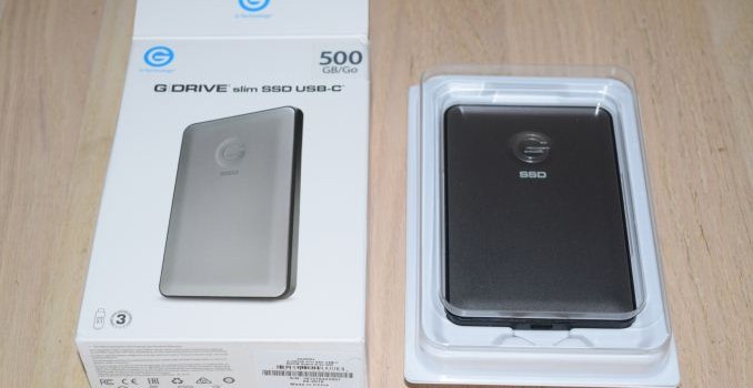
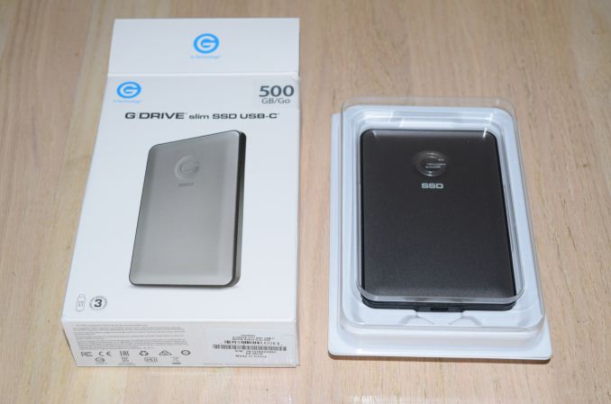
The G-DRVE slim SSD USB-C is a portable USB 3.1 Gen 2 Type-C external SSD. It comes in two capacities – 500GB and 1TB. G-Technology claims speeds of up to 540 MBps, but, in keeping with the usual G-Technology marketing strategy, doesn’t specify much in terms of the internals. This review analyzes the hardware and performance of the 500GB variant for typical DAS workloads

Packaging and Internals

The industrial design of G-Technology products is sleek and attractive, as the primary target is content creators. A majority of those are Mac users who want their peripherals to match the look and feel of Apple hardware. The G-DRIVE slim SSD USB-C is no exception. G-Technology even advertises it as being a good companion to the MacBook. The internal drive also comes pre-formatted in HFS+ for Mac users.

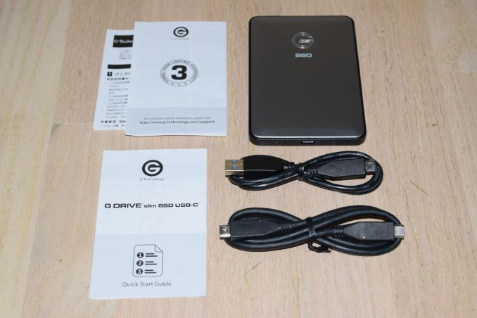
The product is bus-powered. Hence, the supplied material in the package is minimal – just a couple of cables (Type-C to Type-A and Type-C to Type-C) rated for for USB 3.1 Gen 2 speeds. Other than that, we have the usual warranty papers and quick start guide.
The G-Technology G-DRIVE slim SSD USB-C is based on the SanDisk X400 launched earlier this year. It is a TLC-based SSD sporting the Marvell 88SS1074 SSD controller. The first clue to this comes from the CrystalDiskInfo information.
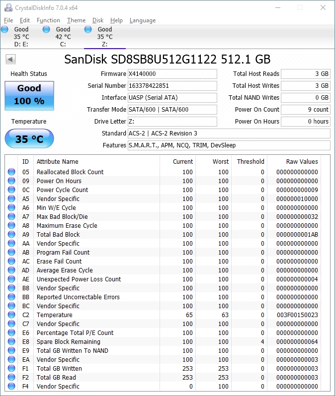
A teardown also reveals the SSD, and, as a bonus, we also see the bridge configuration.

The unit’s Type-C port is well-shielded, and the board reveals the ASMedia ASM1351 SATA to USB 3.1 Gen 2 bridge along with the ASMedia ASM1543 Type-C switch to enable the Type-C port.

Testbed Setup and Testing Methodology

Evaluation of DAS units on Windows is done with the testbed outlined in the table below. For devices with a USB 3.1 Gen 2 (via a Type-C interface) connections (such as the G-DRIVE slim SSD USB-C 500GB that we are considering today), we utilize the USB 3.1 Type-C port enabled by the Intel Alpine Ridge controller. It connects to the Z170 PCH via a PCIe 3.0 x4 link.

AnandTech DAS Testbed Configuration
Motherboard GIGABYTE Z170X-UD5 TH ATX
CPU Intel Core i5-6600K
Memory G.Skill Ripjaws 4 F4-2133C15-8GRR
32 GB ( 4x 8GB)
DDR4-2133 @ 15-15-15-35
OS Drive Samsung SM951 MZVPV256 NVMe 256 GB
SATA Devices Corsair Neutron XT SSD 480 GB
Intel SSD 730 Series 480 GB
Add-on Card None
Chassis Cooler Master HAF XB EVO
PSU Cooler Master V750 750 W
OS Windows 10 Pro x64
Thanks to Cooler Master, GIGABYTE, G.Skill and Intel for the build components

The full details of the reasoning behind choosing the above build components can be found here. The list of DAS units used for comparison purposes is provided below.

  • G-DRIVE slim SSD USB-C 500GB
  • ADATA SE730 250GB
  • ADATA SV620 480GB
  • Netac Z5 512GB
  • Samsung Portable SSD T3 2TB
  • SanDisk Extreme 510 480GB
  • SanDisk Extreme 900 1.92TB

Synthetic Benchmarks – Crystal DiskMark

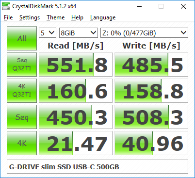
G-Technology claims speeds of up to 540 MBps, and these are backed up by the CrystalDiskMark benchmarks provided below. Unfortunately, despite being better estimate of the real-world performance compared to ATTO, it still suffers from being susceptible to SLC caching when evaluating TLC-based drives. Therefore, it is important to test out real-world scenarios also.

G-DRIVE slim SSD USB-C 500GBADATA SE730 250GBADATA SV620 480GBNetac Z5 512GBSamsung Portable SSD T3 2TBSanDisk Extreme 510 480GBSanDisk Extreme 900 1.92TB
Benchmarks – robocopy and PCMark 8 Storage Bench

Our testing methodology for DAS units also takes into consideration the usual use-case for such devices. The most common usage scenario is transfer of large amounts of photos and videos to and from the unit. The minor usage scenario is importing files directly off the DAS into a multimedia editing program such as Adobe Photoshop.

In order to tackle the first use-case, we created three test folders with the following characteristics:

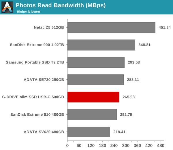
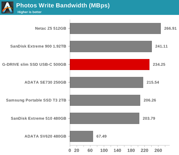
  • Photos: 15.6 GB collection of 4320 photos (RAW as well as JPEGs) in 61 sub-folders
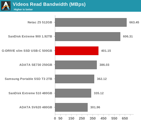
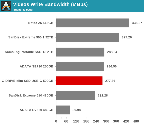
  • Videos: 16.1 GB collection of 244 videos (MP4 as well as MOVs) in 6 sub-folders
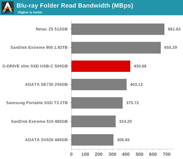
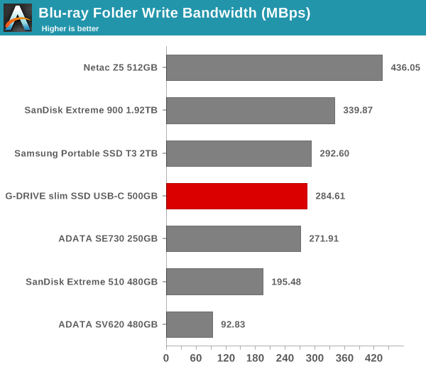
  • BR: 10.7 GB Blu-ray folder structure of the IDT Benchmark Blu-ray (the same that we use in our robocopy tests for NAS systems)
robocopy - Photos Read

robocopy - Photos Write

robocopy - Videos Read

robocopy - Videos Write

robocopy - Blu-ray Folder Read

robocopy - Blu-ray Folder Write

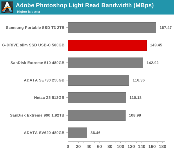
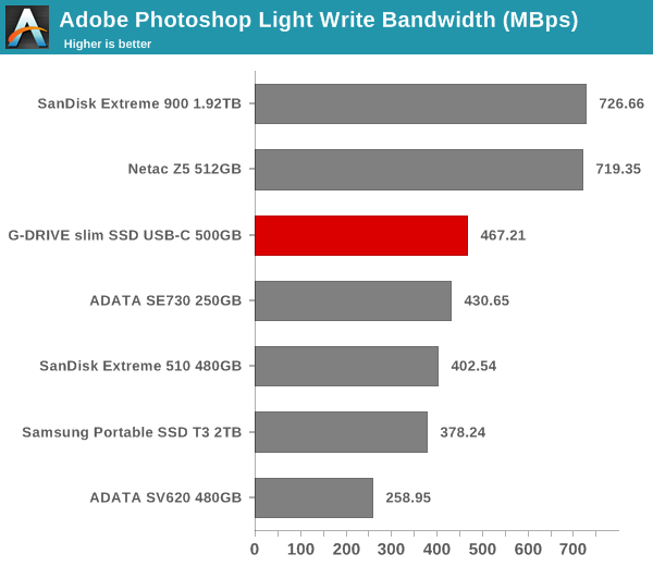
For the second use-case, we take advantage of PC Mark 8’s storage bench. The storage workload involves games as well as multimedia editing applications. The command line version allows us to cherry-pick storage traces to run on a target drive. We chose the following traces.

  • Adobe Photoshop (Light)
  • Adobe Photoshop (Heavy)
  • Adobe After Effects
  • Adobe Illustrator

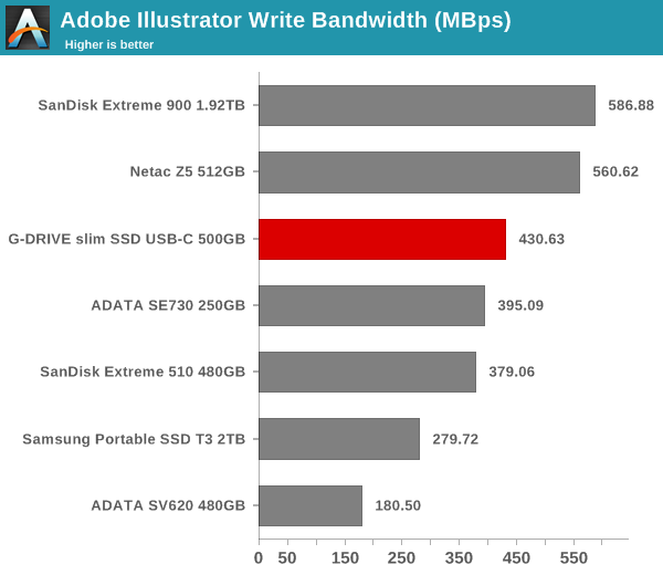
Usually, PC Mark 8 reports time to complete the trace, but the detailed log report has the read and write bandwidth figures which we present in our performance graphs. Note that the bandwidth number reported in the results don’t involve idle time compression. Results might appear low, but that is part of the workload characteristic. Note that the same testbed is being used for all DAS units. Therefore, comparing the numbers for each trace should be possible across different DAS units.
robocopy - Photoshop Light Read

robocopy - Photoshop Light Write

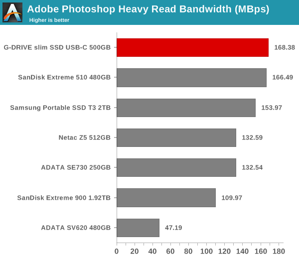
robocopy - Photoshop Heavy Read

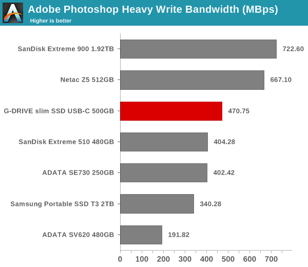
robocopy - Photoshop Heavy Write

robocopy - After Effects Read

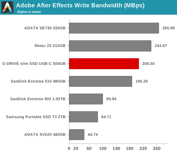
robocopy - After Effects Write

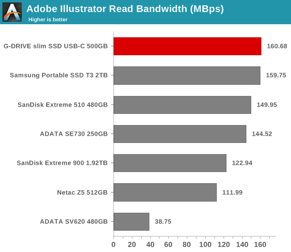
robocopy - Illustrator Read

robocopy - Illustrator Write

The above numbers show that SanDisk’s TLC-based X400 can act as an effective external SSD, but, it still loses out to pure MLC-based SSDs and RAID-ed SSDs for workloads that put heavy stress on the SSD in terms of total traffic. That said, the USB 3.1 Gen 2 interface keeps it ahead of some of the USB 3.0 SSDs with MLC flash.

Performance Consistency

Yet another interesting aspect of these types of units is performance consistency. Aspects that may influence this include thermal throttling and firmware caps on access rates to avoid overheating or other similar scenarios. This aspect is an important one, as the last thing that users want to see when copying over, say, 100 GB of data to the flash drive, is the transfer rate going to USB 2.0 speeds. In order to identify whether the drive under test suffers from this problem, we instrumented our robocopy DAS benchmark suite to record the flash drive’s read and write transfer rates while the robocopy process took place in the background. For supported drives, we also recorded the internal temperature of the drive during the process. The graphs below show the speeds observed during our real-world DAS suite processing. The first three sets of writes and reads correspond to the photos suite. A small gap (for the transfer of the videos suite from the primary drive to the RAM drive) is followed by three sets for the next data set. Another small RAM-drive transfer gap is followed by three sets for the Blu-ray folder.

An important point to note here is that each of the first three blue and green areas correspond to 15.6 GB of writes and reads respectively. Throttling, if any, is apparent within the processing of the photos suite itself. We see absolutely no issues with the thermal performance – The SSD temperature remains below 50C all through, and there is no thermal throttling at play here.

G-DRIVE slim SSD USB-C 500GBADATA SE730 250GBADATA SV620 480GBNetac Z5 512GBSamsung Portable SSD T3 2TBSanDisk Extreme 510 480GBSanDisk Extreme 900 1.92TB
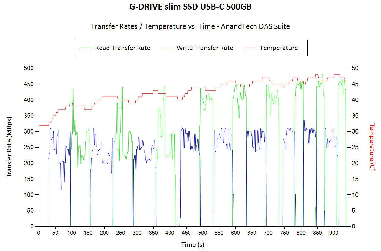
Despite the absence of thermal throttling, we see slight inconsistencies between transfers of the same set of data at different points in time. This is due to the SLC caching implementation and the overhead associated with transferring data from the SLC to TLC segments. That said, the effect is not bad enough for regular users to notice.

Concluding Remarks

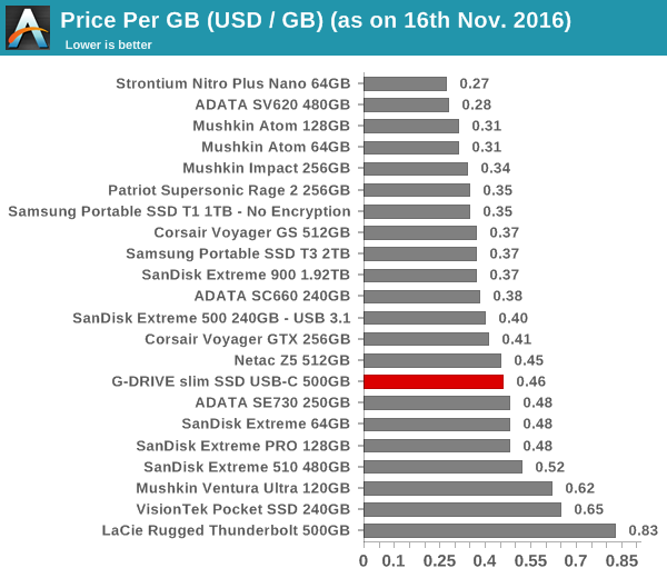
G-Technology’s G-DRIVE slim SSD USB-C is one of the first products in the external DAS space to take advantage of the synergies existing between various companies acquired by Western Digital over the past few years. The USB 3.1 Gen 2 Type-C interface shows that this is a product that looks forward to the future, and appropriately targets people with the latest and greatest computers. Despite that, the pricing is quite reasonable and actually matches several USB flash drives in terms of price per GB.
Price per GB

A minor point of concern is the policy of SanDisk to not implement translation of SCSI Unmap commands to TRIM in their external SSDs. We checked for TRIM support, and Windows reported an error indicating that the volume optimization operation was not supported by the hardware backing the volume.
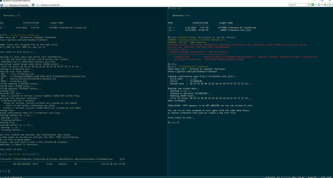
Overall, we are impressed with the performance of the G-DRIVE slim SSD USB-C 500GB version and what it delivers for $230. That said, we would prefer adoption of MLC-based SSDs in this market segment, as TLC presents both long-term performance consistency and durability concerns which get amplified for heavy direct-attached storage workloads.