SSDs


Samsung SSD Update: 48-layer 256Gbit TLC 3D NAND & Three New TLC SSDs Announced

Samsung SSD Update: 48-layer 256Gbit TLC 3D NAND & Three New TLC SSDs Announced

When Samsung took the stage at the 2015 Flash Memory Summit, they admittedly didn’t deliver any bombshell announcements on the scale of the Intel/Micron 3D XPoint surprise, but they still had a lot to talk about.

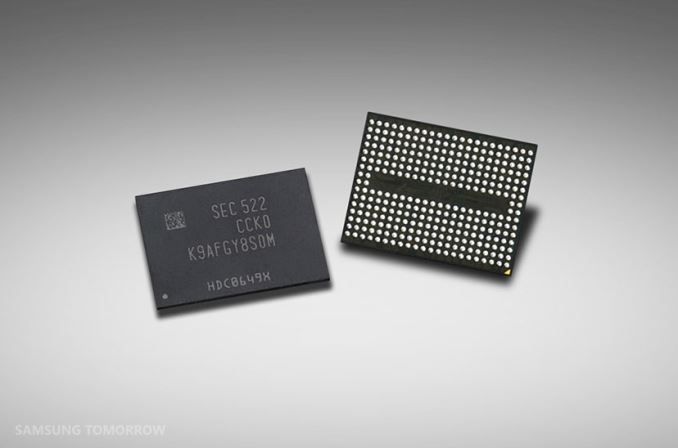
We knew that Samsung’s third generation of V-NAND/3D NAND was on the way with mass production scheduled for the second half of this year. Samsung has now disclosed that mass production is starting this month, and that it’s a 48-layer design with a 256Gb TLC being the first die announced. Samsung’s current second-generation 3D NAND is a 32-layer design available as 128Gb TLC or 128Gb MLC.

With mass production imminent, Samsung has ensured that neither SK Hynix nor the Toshiba/SanDisk joint venture will be able to leapfrog them with their respective 48-layer 3D NAND designs, both scheduled for mass production starting in 2016.

Samsung says the new 256Gb TLC will have about 30% lower power consumption than an equivalent capacity of their current 128Gb TLC, and a switch to a dual-plane organization ensures that one 256Gb die will perform at least as well as a pair of the current 128Gb dies. Density is improved by about 40% while production costs only increased slightly, so price per GB will be going down. At FMS, Samsung is pushing the idea that their 3D NAND TLC is ready to replace MLC for most uses, and they’re optimistic about scaling up their 3D NAND layer count past 100.

New Samsung 48-Layer TLC SSDs
Drive PM953 PM1633 PM1725
Form Factor NVMe over M.2 22110 and 2.5″ 2.5″ SAS 12Gb/s NVMe PCIe HHHL card
Capacities 480GB, 960GB, 1.92TB (2.5″ only) 480GB, 960GB, 1.92TB, 3.84TB 3.2TB, 6.4TB
Sequential Read ? 1,100 MB/s 5,500 MB/s
Sequential Write ? 1,000 MB/s 1,800 MB/s
4kB Random Read IOPS ? 160k 1,000k
4kB Random Write IOPS ? 18k 120k
Endurance Rating ? ? 5 DWPD (6.4 TB model)

Samsung also shared information about three upcoming drives, all using TLC though not necessarily the new 48-layer parts. The PM1633 Enterprise SAS drive was previewed at CES in January and is intended for read-heavy workloads. A follow-on PM1633a model was mentioned to use the new 48-layer TLC to reach 15.36TB capacity, but we don’t have any other information about that update. The PM953 is a enterprise NVMe drive in M.2 or 2.5″ form factors, and is the counterpart to the MLC-based SM951. Of particular interest, the M.2 version is using the M.2 22110 form factor (22mm x 110mm, the maximum length for M.2), with Samsung using the extra space to implement power loss protection.

Meanwhile the PM1725 is a fast multi-TB PCIe expansion card that Samsung intends to use to challenge the assumptions about what uses TLC is suited for. Relatively speaking it appears to be intended for workloads that aren’t very write-heavy, but it still manages 120k IOPS for writes. That just looks small compared to 1M IOPS for reads and a sequential read speed of 5.5GB/s.

All three drives are intended for OEMs, but the PM953 will probably find its way into the retail channel just like the SM951.

Finally, along with Samsung’s new 3D NAND appearing in the afformentioned new drives, it will also be appearing in at least one of their existing drives. The 850 EVO, Samsung’s current consumer TLC drive, will apparently be getting an update to use the new 48-layer TLC, though it’s not clear if this will be new capacities and/or a wholesale NAND update.

Toshiba Brings Through-Silicon Vias to NAND Flash

Toshiba Brings Through-Silicon Vias to NAND Flash

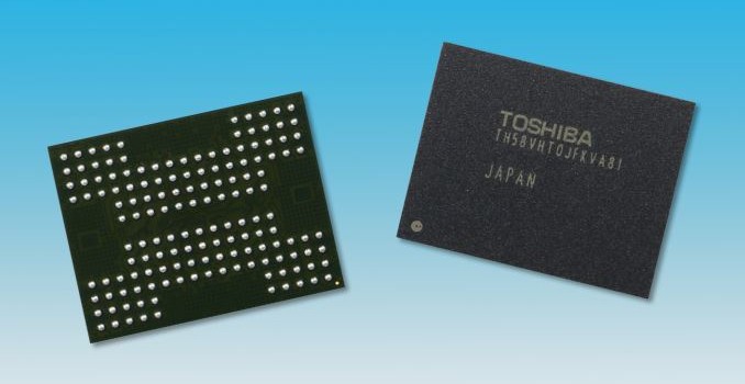
At Flash Memory Summit this week, Toshiba is showing off a NAND flash device packaged using through-silicon vias rather than traditional wire-bonded connections.

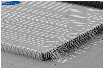
The NAND flash currently on the market is typically produced in the form of a die with a capacity like 128Gb (16GB). The popular SSD form factors don’t have enough surface area to fit dozens of those chips, and SSD controllers don’t have the pin count to connect to that many independently, so several chips are stacked in a single postage-stamp sized package. The traditional way of connecting the individual dies in a stack is to use the same technique as for a single-die package: bonding a thin gold wire between the edge of the die and the package substrate or external pins. The downsides are that it requires a lot of wires and the edges of the dies in the stack need to be exposed somehow, either by staggering them or by putting a spacer between each layer.

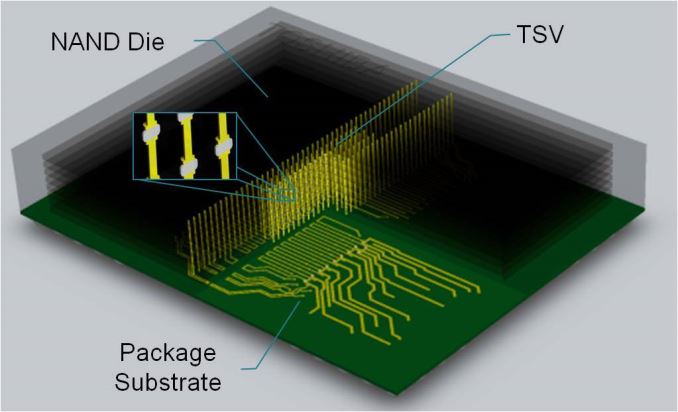
An alternative packaging method is to design the dies to participate in the stacking, by including electrical conductors that penetrate the entire thickness of the silicon die so that they can make contact with the dies above and below it in the stack, essentially tunneling right through each die. These through-silicon vias (TSVs) can then form a shared bus to carry signals from any of the dies in the stack out to the last die, which is the only one with the external connections.

Chip stacking using TSVs requires the dies to be aligned and stacked without spacers, which makes the whole stack a bit more compact. Since TSVs can be placed anywhere on the chip rather than just at the edge, it’s easy to implement a wide data bus and communication within the stack can be very fast or low-power due to the short distances involved. These advantages have been very attractive for packaging DRAM, most notably in the form of the HBM stacks used by AMD’s R9 Fury and R9 Nano video cards.

Toshiba’s demonstration is a 16-high stack of 128Gb dies in a BGA-152 package measuring 14mm by 18mm and 1.9mm thick, and an 8-high stack that’s 1.35mm thick. Those numbers are all typical even for wire-bonded stacks. The speed (1Gb/s) and operating voltages (1.2V for I/O and 1.8V core) are what we would expect from a next-generation NAND interface, but the claimed 50% power reduction is a very nice improvement for a change that leaves the flash memory cells themselves unmodified.

Toshiba hasn’t said whether the dies being stacked are their current 15nm planar NAND or their forthcoming 3D NAND, nor have they said when modules using TSVs will be hitting the market. The most compelling applications would be to use TSVs to stack flash atop a controller chip in an eMMC product or atop an SoC, but the power savings would be appreciated almost everywhere. If the use of TSVs allows economically stacking more than 16 dies, it could enable a dramatic increase in the density of SSDs.

Toshiba Brings Through-Silicon Vias to NAND Flash

Toshiba Brings Through-Silicon Vias to NAND Flash

At Flash Memory Summit this week, Toshiba is showing off a NAND flash device packaged using through-silicon vias rather than traditional wire-bonded connections.

The NAND flash currently on the market is typically produced in the form of a die with a capacity like 128Gb (16GB). The popular SSD form factors don’t have enough surface area to fit dozens of those chips, and SSD controllers don’t have the pin count to connect to that many independently, so several chips are stacked in a single postage-stamp sized package. The traditional way of connecting the individual dies in a stack is to use the same technique as for a single-die package: bonding a thin gold wire between the edge of the die and the package substrate or external pins. The downsides are that it requires a lot of wires and the edges of the dies in the stack need to be exposed somehow, either by staggering them or by putting a spacer between each layer.

An alternative packaging method is to design the dies to participate in the stacking, by including electrical conductors that penetrate the entire thickness of the silicon die so that they can make contact with the dies above and below it in the stack, essentially tunneling right through each die. These through-silicon vias (TSVs) can then form a shared bus to carry signals from any of the dies in the stack out to the last die, which is the only one with the external connections.

Chip stacking using TSVs requires the dies to be aligned and stacked without spacers, which makes the whole stack a bit more compact. Since TSVs can be placed anywhere on the chip rather than just at the edge, it’s easy to implement a wide data bus and communication within the stack can be very fast or low-power due to the short distances involved. These advantages have been very attractive for packaging DRAM, most notably in the form of the HBM stacks used by AMD’s R9 Fury and R9 Nano video cards.

Toshiba’s demonstration is a 16-high stack of 128Gb dies in a BGA-152 package measuring 14mm by 18mm and 1.9mm thick, and an 8-high stack that’s 1.35mm thick. Those numbers are all typical even for wire-bonded stacks. The speed (1Gb/s) and operating voltages (1.2V for I/O and 1.8V core) are what we would expect from a next-generation NAND interface, but the claimed 50% power reduction is a very nice improvement for a change that leaves the flash memory cells themselves unmodified.

Toshiba hasn’t said whether the dies being stacked are their current 15nm planar NAND or their forthcoming 3D NAND, nor have they said when modules using TSVs will be hitting the market. The most compelling applications would be to use TSVs to stack flash atop a controller chip in an eMMC product or atop an SoC, but the power savings would be appreciated almost everywhere. If the use of TSVs allows economically stacking more than 16 dies, it could enable a dramatic increase in the density of SSDs.

SanDisk Announces Second Generation CloudSpeed Ultra SATA Enterprise SSD

SanDisk Announces Second Generation CloudSpeed Ultra SATA Enterprise SSD

At Flash Memory Summit today SanDisk announced the second generation of their CloudSpeed Ultra enterprise drive. This is the sibling to the gen. 2 CloudSpeed Eco that was announced in June.

As with the Eco gen. 2, the Ultra gen. 2 transitions from 19nm to 15nm MLC and brings a reduced endurance rating but increased performance. The Ultra model continues to be geared for mixed read/write workloads while the Eco is for more read-intensive uses.

SanDisk Enterprise SATA SSDs
Drive Ultra gen. 2 Eco gen. 2 Ultra gen. 1
Capacities 400GB, 800GB, 1600GB 480GB, 960GB, 1920GB 100GB, 200GB, 400GB, 800GB
NAND SanDisk 15nm MLC SanDisk 15nm MLC SanDisk 19nm MLC
Sequential Read 530 MB/s 530 MB/s 450 MB/s
Sequential Write 460 MB/s 460 MB/s 400 MB/s
4kB Random Read IOPS 76k 76k 75k
4kB Random Write IOPS 32k 14k 30k
Endurance Rating 1.8 DWPD 0.6 DWPD 3 DWPD

SanDisk is already supplying the CloudSpeed Ultra gen. 2 to several major customers for large-scale deployments and it will be more broadly available later in 2015, where it will be competing against drives like Samsung’s SM863 and Intel’s DC S3610. Pricing will be under $1/GB, but we don’t know by how much. It probably won’t be undercut by Intel’s DC S3610, but to be competitive it will need to be down near Samsung’s $0.66/GB for the SM863.

SanDisk Announces Second Generation CloudSpeed Ultra SATA Enterprise SSD

SanDisk Announces Second Generation CloudSpeed Ultra SATA Enterprise SSD

At Flash Memory Summit today SanDisk announced the second generation of their CloudSpeed Ultra enterprise drive. This is the sibling to the gen. 2 CloudSpeed Eco that was announced in June.

As with the Eco gen. 2, the Ultra gen. 2 transitions from 19nm to 15nm MLC and brings a reduced endurance rating but increased performance. The Ultra model continues to be geared for mixed read/write workloads while the Eco is for more read-intensive uses.

SanDisk Enterprise SATA SSDs
Drive Ultra gen. 2 Eco gen. 2 Ultra gen. 1
Capacities 400GB, 800GB, 1600GB 480GB, 960GB, 1920GB 100GB, 200GB, 400GB, 800GB
NAND SanDisk 15nm MLC SanDisk 15nm MLC SanDisk 19nm MLC
Sequential Read 530 MB/s 530 MB/s 450 MB/s
Sequential Write 460 MB/s 460 MB/s 400 MB/s
4kB Random Read IOPS 76k 76k 75k
4kB Random Write IOPS 32k 14k 30k
Endurance Rating 1.8 DWPD 0.6 DWPD 3 DWPD

SanDisk is already supplying the CloudSpeed Ultra gen. 2 to several major customers for large-scale deployments and it will be more broadly available later in 2015, where it will be competing against drives like Samsung’s SM863 and Intel’s DC S3610. Pricing will be under $1/GB, but we don’t know by how much. It probably won’t be undercut by Intel’s DC S3610, but to be competitive it will need to be down near Samsung’s $0.66/GB for the SM863.