SSDs


Samsung Releases 750 EVO SATA SSD

Samsung Releases 750 EVO SATA SSD

After an accidental leak in November that was spotted by our friends at Tom’s Hardware, the Samsung 750 EVO has now officially launched worldwide. Since the introduction of their first consumer TLC SSD with the 840, Samsung’s consumer/retail SATA SSD lineup has consisted of two product families: the MLC-based Pro drives, and the TLC-based 840 and EVO drives. With the 750 EVO, Samsung is creating a new budget-oriented product line that makes them a participant in the race to the bottom that they had been avoiding by positioning the 850 EVO as a mid-range SSD.

There are several design choices that help minimize the cost of the 750 EVO, aside from the expected choice of TLC over MLC. The MGX controller it borrows from the lower capacity 850 EVOs is a dual-core version of Samsung’s usual triple-core architecture. The 750 EVO will only be available in 120GB and 250GB sizes, so there won’t be any sticker shock of higher capacities and the PCB only needs to be large enough to accommodate the needs of the 250GB model. Both capacities are listed as having 256MB of DRAM, where the 850 EVO 250GB has 512MB of DRAM. But the most significant aspect of the 750 EVO is that it doesn’t use 3D NAND.

It may come as a surprise that the 750 EVO marks a return to planar NAND. Samsung has proudly led the industry in transitioning to 3D NAND, but they haven’t entirely abandoned the development of planar NAND flash. Earlier this month they made two presentations at ISSCC of their R&D accomplishments: one about a 256Gb TLC built on their 48-layer third generation V-NAND process, and one about a 128Gb MLC built on a 14nm process. The 750 EVO uses a 128Gb 16nm TLC, a larger die based on the same process as the 64Gb MLC we found in the SM951.

The 16nm TLC NAND is the successor to Samsung’s 19nm TLC that had a troubled tenure in the 840 EVO. More than a year after launch, 840 EVO owners started reporting degraded read speed when accessing old data that had not been written recently. Samsung acknowledged the issue, then provided a firmware update and Performance Restoration tool less than a month later, but had to issue a second firmware update six months after that. The 750 EVO inherits the results of all the work Samsung did to mitigate the read speed degradation, and there’s no reason to expect it to be any more susceptible than the competition using similarly dense planar TLC built on Toshiba’s 15nm process or Micron’s 16nm process.

Samsung TLC SATA SSD Comparison
Drive 750 EVO 120GB 750 EVO 250GB 850 EVO 120GB 850 EVO 250GB
Controller MGX MGX
NAND Samsung 16nm TLC Samsung 32-layer 128Gbit TLC V-NAND
DRAM 256MB 256MB 256MB 512MB
Sequential Read 540MB/s 540MB/s 540MB/s 540MB/s
Sequential Write 520MB/s 520MB/s 520MB/s 520MB/s
4KB Random Read 94K IOPS 97K IOPS 94K IOPS 97K IOPS
4KB Random Write 88K IOPS 88K IOPS 88K IOPS 88K IOPS
4KB Random Read QD1 10K IOPS 10K IOPS 10K IOPS 10K IOPS
4KB Random Write QD1 35K IOPS 35K IOPS 40K IOPS 40K IOPS
DevSleep Power  6mW 2mW
Slumber Power  50mW 50mW
Active Power (Read/Write) 2.1W / 2.4W (Average) 2.4W / 2.8W (Average) Max 3.7W / 4.4W
Encryption AES-256, TCG Opal 2.0, IEEE-1667 (eDrive) AES-256, TCG Opal 2.0, IEEE-1667 (eDrive)
Endurance 35TB 70TB 75TB
Warranty Three years Five years

The 750 EVO’s performance specifications are almost identical to the 850 EVOs of the same capacity. The 4kB random write latency is a little bit worse, but read speeds are the same and any other differences in the write performance of the 15nm flash are masked by the SLC write cache. The reduced warranty period of three years is typical for this product segment, and while the write endurance specifications may look quite low, they’re sufficient given the capacity and intended use. It’s nice to see that the 750 EVO keeps the encryption capabilities fully enabled, as many budget drives lack hardware encryption support.

Given the aforementioned similarities with the 850 EVO, it should come as no surprise that the 750 EVO is in part a replacement. The previously announced and now imminent migration to Samsung’s 48-layer V-NAND won’t apply to the 120GB 850 EVO, as the 256Gb per die capacity would mean building a drive with only four flash chips. That is undesirable from both a performance standpoint and from a packaging standpoint—Samsung will otherwise have no reason to stack fewer than 8 dies per package.

A few online retailers are listing the 750 EVO already, albeit with limited or no stock. The MSRP of $54.99 for the 120GB model and $74.99 for the 250GB model is about $10 cheaper than what the 850 EVO is currently going for, and any sales below MSRP will make for a very competitive price.

Samsung Releases 750 EVO SATA SSD

Samsung Releases 750 EVO SATA SSD

After an accidental leak in November that was spotted by our friends at Tom’s Hardware, the Samsung 750 EVO has now officially launched worldwide. Since the introduction of their first consumer TLC SSD with the 840, Samsung’s consumer/retail SATA SSD lineup has consisted of two product families: the MLC-based Pro drives, and the TLC-based 840 and EVO drives. With the 750 EVO, Samsung is creating a new budget-oriented product line that makes them a participant in the race to the bottom that they had been avoiding by positioning the 850 EVO as a mid-range SSD.

There are several design choices that help minimize the cost of the 750 EVO, aside from the expected choice of TLC over MLC. The MGX controller it borrows from the lower capacity 850 EVOs is a dual-core version of Samsung’s usual triple-core architecture. The 750 EVO will only be available in 120GB and 250GB sizes, so there won’t be any sticker shock of higher capacities and the PCB only needs to be large enough to accommodate the needs of the 250GB model. Both capacities are listed as having 256MB of DRAM, where the 850 EVO 250GB has 512MB of DRAM. But the most significant aspect of the 750 EVO is that it doesn’t use 3D NAND.

It may come as a surprise that the 750 EVO marks a return to planar NAND. Samsung has proudly led the industry in transitioning to 3D NAND, but they haven’t entirely abandoned the development of planar NAND flash. Earlier this month they made two presentations at ISSCC of their R&D accomplishments: one about a 256Gb TLC built on their 48-layer third generation V-NAND process, and one about a 128Gb MLC built on a 14nm process. The 750 EVO uses a 128Gb 16nm TLC, a larger die based on the same process as the 64Gb MLC we found in the SM951.

The 16nm TLC NAND is the successor to Samsung’s 19nm TLC that had a troubled tenure in the 840 EVO. More than a year after launch, 840 EVO owners started reporting degraded read speed when accessing old data that had not been written recently. Samsung acknowledged the issue, then provided a firmware update and Performance Restoration tool less than a month later, but had to issue a second firmware update six months after that. The 750 EVO inherits the results of all the work Samsung did to mitigate the read speed degradation, and there’s no reason to expect it to be any more susceptible than the competition using similarly dense planar TLC built on Toshiba’s 15nm process or Micron’s 16nm process.

Samsung TLC SATA SSD Comparison
Drive 750 EVO 120GB 750 EVO 250GB 850 EVO 120GB 850 EVO 250GB
Controller MGX MGX
NAND Samsung 16nm TLC Samsung 32-layer 128Gbit TLC V-NAND
DRAM 256MB 256MB 256MB 512MB
Sequential Read 540MB/s 540MB/s 540MB/s 540MB/s
Sequential Write 520MB/s 520MB/s 520MB/s 520MB/s
4KB Random Read 94K IOPS 97K IOPS 94K IOPS 97K IOPS
4KB Random Write 88K IOPS 88K IOPS 88K IOPS 88K IOPS
4KB Random Read QD1 10K IOPS 10K IOPS 10K IOPS 10K IOPS
4KB Random Write QD1 35K IOPS 35K IOPS 40K IOPS 40K IOPS
DevSleep Power  6mW 2mW
Slumber Power  50mW 50mW
Active Power (Read/Write) 2.1W / 2.4W (Average) 2.4W / 2.8W (Average) Max 3.7W / 4.4W
Encryption AES-256, TCG Opal 2.0, IEEE-1667 (eDrive) AES-256, TCG Opal 2.0, IEEE-1667 (eDrive)
Endurance 35TB 70TB 75TB
Warranty Three years Five years

The 750 EVO’s performance specifications are almost identical to the 850 EVOs of the same capacity. The 4kB random write latency is a little bit worse, but read speeds are the same and any other differences in the write performance of the 15nm flash are masked by the SLC write cache. The reduced warranty period of three years is typical for this product segment, and while the write endurance specifications may look quite low, they’re sufficient given the capacity and intended use. It’s nice to see that the 750 EVO keeps the encryption capabilities fully enabled, as many budget drives lack hardware encryption support.

Given the aforementioned similarities with the 850 EVO, it should come as no surprise that the 750 EVO is in part a replacement. The previously announced and now imminent migration to Samsung’s 48-layer V-NAND won’t apply to the 120GB 850 EVO, as the 256Gb per die capacity would mean building a drive with only four flash chips. That is undesirable from both a performance standpoint and from a packaging standpoint—Samsung will otherwise have no reason to stack fewer than 8 dies per package.

A few online retailers are listing the 750 EVO already, albeit with limited or no stock. The MSRP of $54.99 for the 120GB model and $74.99 for the 250GB model is about $10 cheaper than what the 850 EVO is currently going for, and any sales below MSRP will make for a very competitive price.

Micron 3D NAND Status Update

Micron 3D NAND Status Update

Update: We’ve got some more information and diagrams from Micron’s Winter Analyst Conference earlier today.

After samples of their upcoming 3D NAND were sighted in the wild at CES, Micron has taken the time to provide some details about the flash memory and their plans for it. A lot of this is a recap of information we’ve previously covered, but we’ve got some new details and a better idea of the roadmap for the future.

The entire flash memory industry has shifted focus to the devlopment of 3D NAND flash memory as the replacement for planar NAND flash memory. Samsung took an aggressive approach and has enjoyed some great success with their V-NAND branded 3D NAND, but it hasn’t been an entirely trouble-free transition. Micron has been more conservative both in technology and timing, but they plan on having a strong competitor on the market later this year.

Micron’s first generation 3D NAND takes the form of a 256Gb MLC die and a 384Gb TLC die (compare with their 128Gb 16nm MLC and TLC). At a high level, the die will be partitioned into four separate planes, compared to two planes for most competing NAND. A 480GB drive using the four-plane 256Gb dies will have access to approximately the same amount of parallelism as a 480GB drive using two-plane 128Gb dies, so this capacity jump won’t bring the performance drops that have tarnished some NAND process shrinks.

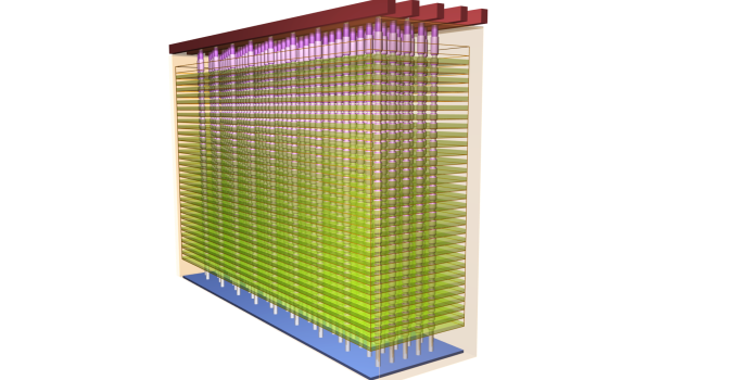
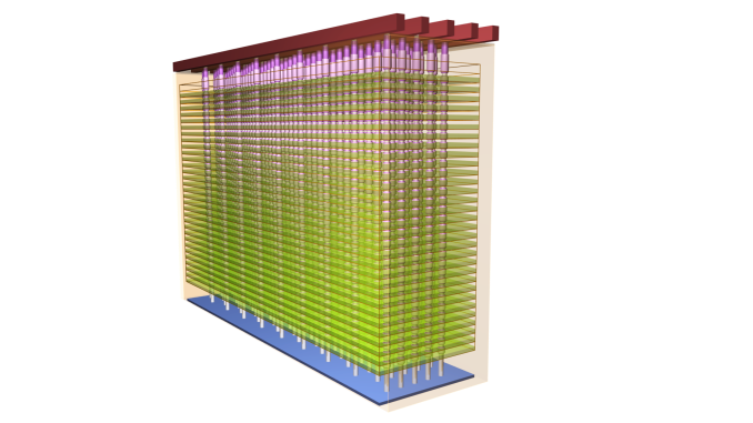
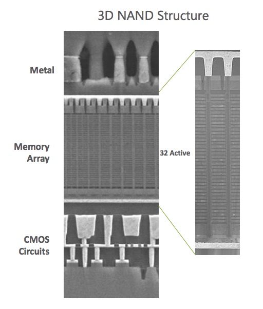
The key development that allows Micron to produce a four-plane die without inflating die size and cost relative to the two-plane competition is that they’ve layered much of the required additional circuitry under the 3D flash array, instead of sitting alongside. Micron says that their “CMOS Under the Array” design puts more than 75% of the logic (things like address decoding and page buffers) under the flash memory. It doesn’t make the additional segmentation of the four-plane design entirely free, but it allows it to be a very cost effective performance optimization. This is still planar CMOS logic, not any kind of 3D or stacked logic; it’s just got some metal interconnect layers and the flash array piled on top.

On a smaller scale, the 3D NAND will have a page size of 16kB and erase block sizes of 16MB for the MLC and 24MB for the TLC. Because CPUs and filesystems are still mostly dealing with 4kB chunks, Micron has included a partial page read capability that allows for a 4kB read to be done a bit faster and with about half the power of a full 16kB page read. This helps offset some of the penalty the larger page size can have on random 4kB read performance. The large erase block sizes won’t have much of a direct impact on performance and are a necessary efficiency measure: erasing requires charge pumps to produce higher voltages than reads or writes use, and it’s a slower and more power-hungry operation. If you’re going to fire up that extra circuitry and block access to the entire plane for 1ms or more, you might as well erase a usefully large amount of flash.

For the architecture of the individual memory cells, we have nothing new to report. Intel and Micron are alone in their decision to stick with floating-gate flash technology instead of transitioning to charge-trap flash. We’ve previously explained how the technologies differ and what kinds of advantages the manufacturers want to reap from the change. The cost is that the design process involves different tradeoffs that are not as thoroughly explored and understood as the dynamics of floating-gate flash, and for now Micron is sticking with what they know. Micron’s 3D NAND might not have the best write endurance, but they’re expecting to have an advantage in data retention time for healthy flash. They aren’t providing exact numbers, but they’re estimating that drives relying on simpler BCH ECC can get effective program-erase cycle lifetimes in the thousands and drives with LDPC will have effective cycle counts of tens of thousands. Once the process has matured it should exceed their 20nm planar NAND’s write endurance.

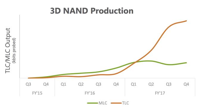
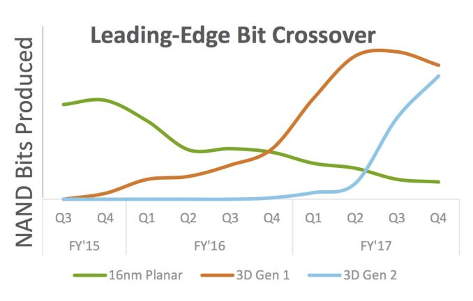
The first 3D NAND Micron has ready for the market will produced to the endurance standards for client drives, with enterprise-grade 3D NAND following later. The MLC is currently a few weeks ahead of the TLC in the qualification process, but given the state of the client SSD market the TLC will be the more popular product and will overtake the MLC in volume produced within a few months of 3D NAND drives hitting the market. Overall their 3D NAND will comprise a majority of their flash output on a per-GB basis by the second half of 2016. Micron is sampling drives with 3D NAND to partners this month and is planning for general availability in June. Other drive vendors using Micron’s NAND will be on similar release schedules.

Micron hasn’t announced any specific drive models, but they’ve given a general roadmap that is unsurprising. Consumer and client products will come during the middle of the year, with the capacity and cost improvements allowing for things like 2TB 2.5″ drives and 1TB single-sided M.2 drives. Toward the end of 2016 and into 2017 we’ll see enterprise products such as very high capacity (8TB+) drives and updates in the existing product segments for SAS and PCIe drives.

Looking further to the future, Micron gave a presentation last week at the IEEE International Solid-State Circuits Conference entitled “A 768Gb 3b/cell 3D-Floating-Gate NAND Flash Memory”. This was more about bragging about their R&D in an academic context than announcing any concrete future product plans, but it does represent the most likely successor to their first-generation 3D NAND. The chip in question provides a whopping 768Gb (96GB) capacity when operated as TLC, and 512Gb (64GB) as MLC. The die size is about the same as their 32-layer 384Gb TLC, the areal bit density is almost doubled, and most of the other details are the same—implying that the layer count has probably increased, though Micron isn’t saying how many layers it uses. If Micron has plans to switch to charge-trap flash they’re keeping it under wraps for now, and any such transition isn’t imminent. The second-generation 3D NAND will start production in their Singapore fab this summer, and volume will be ramping up around the end of 2016 (during the second quarter of their fiscal year 2017). Micron predicts their second-generation 3D NAND will be at least 30% cheaper per Gb than the first generation, which they report to be at least 25% cheaper than their 16nm planar NAND.


Plextor Introduces M6S Plus SSDs with Toshiba’s 15nm MLC NAND

Plextor Introduces M6S Plus SSDs with Toshiba’s 15nm MLC NAND

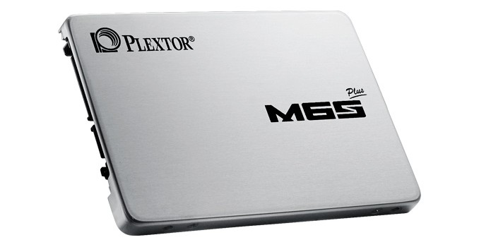
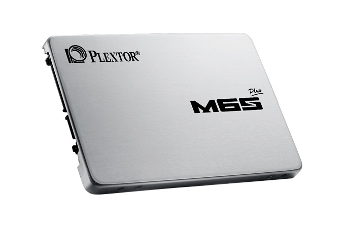
Plextor this week introduced its M6S Plus SSDs that use Toshiba’s latest MLC NAND flash memory as well as a proven controller from Marvell. The new SSDs offer the same level of performance and the same feature set as their predecessors, the M6S drives introduced in 2014. The drives offer read and write speeds expected from SATA SSDs as well as Plextor’s technologies designed to guarantee high reliability and high performance after long periods of usage.

The new Plextor M6S Plus SSDs are based on the Marvell 88SS9188 controller as well as Toshiba’s newest 15 nm MLC NAND. Earlier Plextor offered M6S solid-state drives based on the same controller chip, but featured Toshiba’s older 19 nm MLC NAND. Apparently, Plextor will have to switch to a new type of NAND as manufacturers tend to decrease production of memory using outdated process technologies. The new drives are offered in 2.5-inch/7 mm form-factor and use the SATA-6 Gb/s interface.

The Plextor M6S Plus SSDs feature 128 GB, 256 GB and 512 GB capacities. They are rated to offer maximum sequential read/write speed of up to 520/440MB/s. Maximum random 4K read/write speed declared by Plextor is 94K/80K IOPS (input/output operations per second). It is noteworthy that to guarantee high performance, the new SSDs from Plextor are equipped with up to 768 MB of DDR3 DRAM-based cache.

Specifications of Plextor M6S Plus SSDs
  PX-128M6S+ PX-256M6S+ PX-512M6S+
Capacity 128 GB 256 GB 512 GB
Controller Marvell 88SS9188
NAND Toshiba, MLC 15nm
Cache 256 MB DDR3 512 MB DDR3 768 MB DDR3
Sequential Read Speed up to 520 MB/s up to 520 MB/s up to 520 MB/s
Sequential Write Speed up to 300 MB/s up to 420 MB/s up to 440 MB/s
4K Random Read up to 88K IOPS up to 90K IOPS up to 94K IOPS
4K Random Write up to 75K IOPS up to 80K IOPS up to 80K IOPS
Form-Factor 2.5-inch/7mm
Interface SATA-6 Gbps

Notably, the performance specifications for the new M6S Plus lineup is identical to that of the previous M6S series. As Plextor didn’t switch controllers and didn’t switch NAND vendors, this means that they most likely are just using 15nm NAND as a drop-in replacement for their existing designs, and there won’t be any generational performance changes such as using fewer, higher capacity NAND dies. This has been an issue in the past when vendors have switched to newer generation NAND and labeled the resulting product under an old brand, so kudos to Plextor for making the 15nm drives their own line anyhow.

However while the switch to 15nm NAND doesn’t impact performance, it’s unclear whether the endurance of the newer M6S Plus series has been impacted, as the company hasn’t published any endurance figures for the new drives. Typically, MLC NAND produced using thinner fabrication process has lower P/E cycle rating compared to flash memory produced using thicker manufacturing technology. The 19nm M6S series was rated for 72TB, so it will be interesting to see where the M6S Plus ends up.

Moving on, contemporary Plextor’s SSDs also ship with the company’s PlexTurbo RAM caching technology, which is aimed to improve performance beyond limitations of SATA-6Gb/s interface. The caching works like RAM disk, hence, uses system memory. The M6S Plus also supports TrueSpeed (supposed to guarantee maximum performance over long usage periods) and TrueProtect (a multi-layer error correction capability) firmware-based technologies developed by the company.

Finally, exact MSRPs of the Plextor M6S Plus drives are unknown. However, Amazon plans to start selling the 128 GB version for $62, the 256 GB model for $91 and the 512 GB flavour for $166 shortly.

The Plextor M6S Plus SSDs appear to be pretty affordable, in fact, even more affordable than their predecessors. Apparently, the recent price drops of NAND flash helped Plextor to build inexpensive SSDs based on 15 nm MLC NAND flash from Toshiba, which is not a bad choice, considering the fact that the company managed to maintain performance numbers of the M6S. By contrast, many of Plextor’s rivals are using TLC NAND to make cheap SSDs.

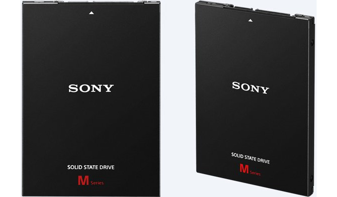
Sony Enters SSD Market with Phison S10-Based SLW-M Series

Sony Enters SSD Market with Phison S10-Based SLW-M Series

Sony-Asia this month introduced its first own-brand solid-state drives that it will sell in retail. The decision to start selling consumer SSDs is completely unexpected because Sony has been trying to focus solely on highly profitable and less competitive businesses in the recent years, whereas the competition in the market of consumer storage is fierce. Initially, the company will sell only two SSD models, which means that it is trying to test a new business rather than to become a leader on the market.

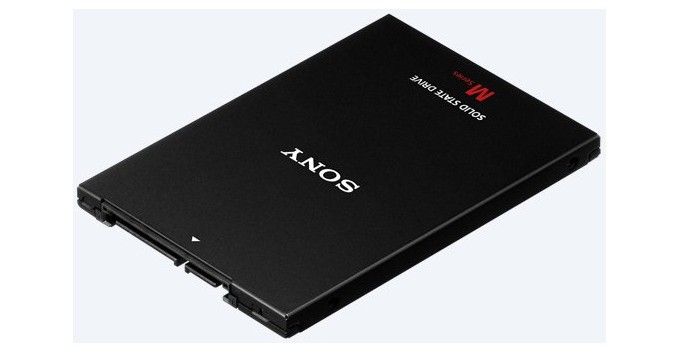
Sony’s SLW-M SSDs come in 2.5-inch/7 mm form-factor (a special bracket to install the drives into 9.5-mm bays is included) and feature 240 GB (SLW-MG2) or 480 GB (SLW-MG4) capacities. The drives use SATA-6 Gbps interface and hence Sony can address the vast majority of desktop and laptop PCs with its first-gen SSDs. According to Sony, the SLW-M solid-state drives feature up to 560 MB/s sequential write speed and up to 530 MB/s sequential write speed. Each drives comes equipped with the Acronis True image 2015 and Sony SSD ToolBox software for managing and saving your data.

The Sony SLW-M SSDs are based on the Phison PS3110-S10 controller as well as Toshiba’s TLC flash memory, according to images published by DIYPC.hk web-site. The SLW-MG2 solid-state drive from Sony features 128 MB DDR3 buffer made by Nanya. Usage of TLC NAND indicates that Sony’s SLW-M are entry-level client solid-state solutions that do not cost a lot to make and are not supposed to be expensive, and based on the specifications listed it’s a reasonable guess that performance will be near the similarly-built low-end OCZ Trion 100 series.

Meanwhile with the Sony drives it’s worth noting that Phison not only sells controller chips to makers of SSDs, but actual turnkey solutions, which include ASICs, firmware, reference designs of solid-state drives, software, and so on, and this appears to be what Sony is doing. The PCB design of Sony’s SLW-M resembles that of Kingston’s HyperX Savage, Corsair’s Neutron XT and Patriot’s Ignite, while Sony’s SSD ToolBox is rebranded Phison ToolBox.

Many new SSD suppliers acquire Phison’s turnkey solutions in order to produce own drives and find out whether they can successfully sell such products to their customers via their sales channels. For example, Zotac last year introduced its first SSDs powered by Phison’s PS3110-S10 controllers and Toshiba’s MLC NAND flash memory.

Sony’s SSD plans are not completely clear. At present, the company only sells its solid-state drives in select Asian markets and it is unknown whether Sony has plans to offer similar products in the U.S. or Europe. Nonetheless, it is noteworthy that the company, which has been withdrawing from commoditized markets for years, is trying to sell its own SSDs. Nowadays solid-state drives are not as cheap as HDDs, but in the entry level the competition is fierce and margins are low.