SSDs


Everspin Announces New MRAM Products And Partnerships

Everspin Announces New MRAM Products And Partnerships

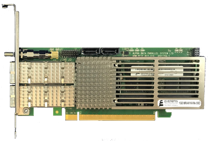
Magnetoresistive RAM manufacturer Everspin has announced their first MRAM-based storage products and issued two other press releases about recent accomplishments. Until now, Everspin’s business model has been to sell discrete MRAM components, but they’re introducing a NVMe SSD based on their MRAM. Everspin’s MRAM is one of the highest-performing and most durable non-volatile memory technologies on the market today, but its density and capacity falls far short of NAND flash, 3D XPoint, and even DRAM. As a result, use of MRAM has largely been confined to embedded systems and industrial computing that need consistent performance and high reliability, but have very modest capacity requirements. MRAM has also seen some use as a non-volatile cache or configuration memory in some storage array controllers. The new nvNITRO family of MRAM drives is intended to be used as a storage accelerator: a high-IOPS low-latency write cache or transaction log, with performance exceeding that of any single-controller drive based on NAND flash.

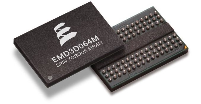
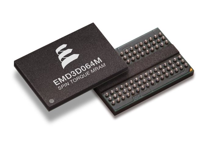
Everspin’s current generation of spin-torque MRAM has a capacity of 256Mb per die with a DDR3 interface (albeit with very different timings from JEDEC standard for DRAM). The initial nvNITRO products will use 32 or 64 MRAM chips to offer capacities of 1GB or 2GB on a PCIe 3 x8 card. MRAM has high enough endurance that the nvNITRO does not need to perform any wear leveling, which allows for a drastically simpler controller design and means performance does not degrade over time or as the drive is filled up—the nvNITRO does not need any large spare area or overprovisioning. Read and write performance are also nearly identical, while flash memory suffers from much slower writes than reads, which forces flash-based SSDs to buffer and combine writes in order to offer good performance. Everspin did not have complete performance specifications available at time of writing, but the numbers they did offer are very impressive: 6µs overall latency for 4kB transfers (compared to 20µs for the Intel SSD DC P3700), and 1.5M IOPS (4kB) at QD32 (compared to 1.2M IOPS read/200k IOPS write for the HGST Ultrastar SN260). The nvNITRO does rely somewhat on higher queue depths to deliver full performance, but it is still able to deliver over 1M IOPS at QD16, around 800k IOPS at QD8, and QD1 performance is around 175k IOPS read/150k IOPS write. MRAM supports fine-grained access, so the nvNITRO performs well even with small transfer sizes: Everspin has hit 2.2M IOPS for 512B transfers, although that is not an official performance specification or measurement from the final product.

As part of today’s announcements, Everspin is introducing MRAM support for Xilinx UltraScale FPGAs in the form of scripts for Xilinx’s Memory Interface Generator tool. This will allow customers to integrate MRAM into their designs as easily as they would use SDRAM or SRAM. The nvNITRO drives are a demonstration of this capability, as the SSD controller is implemented on a Xilinx FPGA. The FPGA provides the PCIe upstream link as a standard feature, the memory controller is Everspin’s new and Everspin has developed a custom NVMe implementation to take advantage of the low latency and simple management afforded by MRAM. Everspin claims a 30% performance advantage over an unspecified NVRAM drive based on battery-backed DRAM, and attributes it primarily to their lightweight NVMe protocol implementation. In addition to NVMe, the nvNITRO can be configured to allow all or part of the memory to be directly accessible for memory-mapped IO, bypassing the protocol overhead of NVMe.


The initial version of the nvNITRO is built with an off-the-shelf FPGA development board and mounts the MRAM on a pair of SO-DIMMs. Later this year Everspin will introduce new denser versions on a custom PCIe card, as well as M.2 drives and 2.5″ U.2 using a 15mm height to accommodate two stacked PCBs. By the end of the year, Everspin will be shipping their next generation 1Gb ST-MRAM with a DDR4 interface, and the nvNITRO will use that to expand to capacities of up to 16GB in the PCIe half-height half-length card form factor, 8GB in 2.5″ U.2, and at least 512MB for M.2.

Everspin has not announced pricing for the nvNITRO products. The first generation nvNITRO products are currently sampling to select customers and will be for sale in the second quarter of this year, primarily through storage vendors and system integrators as a pre-installed option.

New Design Win For Current MRAM

Everspin is also announcing another design win for their older field-switched MRAM technology. JAG Jakob Ltd is adopting Everspin’s 16Mb MRAM parts for their PdiCS process control systems, with MRAM serving as both working memory and code storage. These systems have extremely strict uptime requirements, hard realtime performance requirements and service lifetimes of up to 20 years; there are very few memory technologies on the market that can satisfy all of those requirements. Everspin will continue to develop their line of MRAM devices that compete against SRAM and NOR flash even as their higher-capacity offerings adopt DRAM-like interfaces.

Everspin Announces New MRAM Products And Partnerships

Everspin Announces New MRAM Products And Partnerships

Magnetoresistive RAM manufacturer Everspin has announced their first MRAM-based storage products and issued two other press releases about recent accomplishments. Until now, Everspin’s business model has been to sell discrete MRAM components, but they’re introducing a NVMe SSD based on their MRAM. Everspin’s MRAM is one of the highest-performing and most durable non-volatile memory technologies on the market today, but its density and capacity falls far short of NAND flash, 3D XPoint, and even DRAM. As a result, use of MRAM has largely been confined to embedded systems and industrial computing that need consistent performance and high reliability, but have very modest capacity requirements. MRAM has also seen some use as a non-volatile cache or configuration memory in some storage array controllers. The new nvNITRO family of MRAM drives is intended to be used as a storage accelerator: a high-IOPS low-latency write cache or transaction log, with performance exceeding that of any single-controller drive based on NAND flash.

Everspin’s current generation of spin-torque MRAM has a capacity of 256Mb per die with a DDR3 interface (albeit with very different timings from JEDEC standard for DRAM). The initial nvNITRO products will use 32 or 64 MRAM chips to offer capacities of 1GB or 2GB on a PCIe 3 x8 card. MRAM has high enough endurance that the nvNITRO does not need to perform any wear leveling, which allows for a drastically simpler controller design and means performance does not degrade over time or as the drive is filled up—the nvNITRO does not need any large spare area or overprovisioning. Read and write performance are also nearly identical, while flash memory suffers from much slower writes than reads, which forces flash-based SSDs to buffer and combine writes in order to offer good performance. Everspin did not have complete performance specifications available at time of writing, but the numbers they did offer are very impressive: 6µs overall latency for 4kB transfers (compared to 20µs for the Intel SSD DC P3700), and 1.5M IOPS (4kB) at QD32 (compared to 1.2M IOPS read/200k IOPS write for the HGST Ultrastar SN260). The nvNITRO does rely somewhat on higher queue depths to deliver full performance, but it is still able to deliver over 1M IOPS at QD16, around 800k IOPS at QD8, and QD1 performance is around 175k IOPS read/150k IOPS write. MRAM supports fine-grained access, so the nvNITRO performs well even with small transfer sizes: Everspin has hit 2.2M IOPS for 512B transfers, although that is not an official performance specification or measurement from the final product.

As part of today’s announcements, Everspin is introducing MRAM support for Xilinx UltraScale FPGAs in the form of scripts for Xilinx’s Memory Interface Generator tool. This will allow customers to integrate MRAM into their designs as easily as they would use SDRAM or SRAM. The nvNITRO drives are a demonstration of this capability, as the SSD controller is implemented on a Xilinx FPGA. The FPGA provides the PCIe upstream link as a standard feature, the memory controller is Everspin’s new and Everspin has developed a custom NVMe implementation to take advantage of the low latency and simple management afforded by MRAM. Everspin claims a 30% performance advantage over an unspecified NVRAM drive based on battery-backed DRAM, and attributes it primarily to their lightweight NVMe protocol implementation. In addition to NVMe, the nvNITRO can be configured to allow all or part of the memory to be directly accessible for memory-mapped IO, bypassing the protocol overhead of NVMe.


The initial version of the nvNITRO is built with an off-the-shelf FPGA development board and mounts the MRAM on a pair of SO-DIMMs. Later this year Everspin will introduce new denser versions on a custom PCIe card, as well as M.2 drives and 2.5″ U.2 using a 15mm height to accommodate two stacked PCBs. By the end of the year, Everspin will be shipping their next generation 1Gb ST-MRAM with a DDR4 interface, and the nvNITRO will use that to expand to capacities of up to 16GB in the PCIe half-height half-length card form factor, 8GB in 2.5″ U.2, and at least 512MB for M.2.

Everspin has not announced pricing for the nvNITRO products. The first generation nvNITRO products are currently sampling to select customers and will be for sale in the second quarter of this year, primarily through storage vendors and system integrators as a pre-installed option.

New Design Win For Current MRAM

Everspin is also announcing another design win for their older field-switched MRAM technology. JAG Jakob Ltd is adopting Everspin’s 16Mb MRAM parts for their PdiCS process control systems, with MRAM serving as both working memory and code storage. These systems have extremely strict uptime requirements, hard realtime performance requirements and service lifetimes of up to 20 years; there are very few memory technologies on the market that can satisfy all of those requirements. Everspin will continue to develop their line of MRAM devices that compete against SRAM and NOR flash even as their higher-capacity offerings adopt DRAM-like interfaces.
NGD Launches Catalina: a 24 TB PCIe 3.0 x4 SSD with 3D TLC NAND

NGD Launches Catalina: a 24 TB PCIe 3.0 x4 SSD with 3D TLC NAND

NGD Systems this week announced its first SSD that also happens to be one of the highest capacity drives in the industry. The NGD Catalina uses a proprietary controller as well as up to 24 TB of Micron’s 3D TLC NAND memory and apart from capacity, its key feature is a relatively low power consumption.

Before we jump to the Catalina SSD, it makes sense to talk about NGD Systems (formerly known as NxGn Data) itself. The company was founded in June 2013 by a group of people who previously developed SSDs at companies like Western Digital, STEC and Memtech, with the corporate aim to develop drives for enterprise and hyperscale applications. Back in 2014, the company disclosed that its primary areas of interest were LDPC, advanced signal processing, software-defined media channel architecture and in-storage computation capability. NGD has been developing various proprietary technologies behind the Catalina since its inception and the SSD is a culmination of their work.

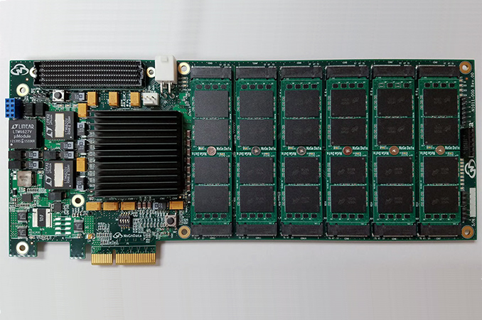
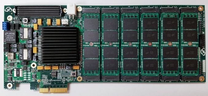
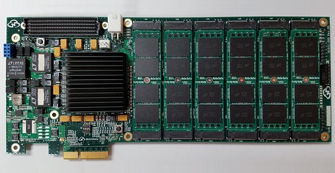
The NGD Catalina is a large add-in-card with a PCIe 3.0 x4 interface that also supports a Mezzanine connector. Rather than have the NAND on the main card, instead the card uses multiple M.2 modules with Micron’s 3D TLC NAND. The 24 TB version of Catalina carries 12 of such modules, whereas lower capacity SKUs will use a fewer modules. According to NGD, the Catalina consumes only 0.65 W of power per Terabyte (which means ~15.6 W for the 24 TB SSD), but the card still has a 4-pin auxiliary power connector.

Keeping in mind that the SSD has a PCIe 3.0 x4 interface, the peak read/write performance of the drive is limited to 3.9 GB/s. Meanwhile, NGD does not disclose official performance or endurance numbers for the Catalina SSD, but only says that the drive is optimized for read-intensive applications.

The NGD Catalina is based on the company’s proprietary ASIC controller which performs LDPC ECC and enables NGD’s patented Elastic FTL (Flash Translation Layer) algorithm, which we believe is for software defined media channels and is claimed said to lower power consumption of SSDs. We do not know anything about the architecture of the controller used by the Catalina, but back in 2014 the company said (according to EETimes) that its controller used ARM’s Cortex-A9 cores (UPDATE3/5: the new controller uses the A53) that ran a micro-OS based on Linux to perform the usual tasks as well as in-storage (In-Situ) computing.

In-Situ is One of the technologies that NGD has been evangelizing since its establishment. In-storage processing moves a compute function closer to the data and allows executing an app on the drive through the Cortex A9s. This concept makes particular sense for various applications that have to search through and analyze large amounts of data (e.g., Big Data) because it eliminates in-device network bottlenecks (there is no need to transfer all the data to the CPU if basic search functions can be done on the drive). The In-Situ paradigm does not abolish host CPUs or operating systems that make requests and manage operations, but it reduces loads on data buses, network, and CPUs to improve performance and reduce power consumption of data centers. It is not stated if the NGD Catalina supports In-Situ though.

The NGD Catalina is being qualified at various OEMs and is available at various capacity points to interested parties. The company does not talk about exact pricing of its drives because a lot depends on actual capacity points as well as volumes of the SSDs acquired.

Related Reading:

NGD Launches Catalina: a 24 TB PCIe 3.0 x4 SSD with 3D TLC NAND

NGD Launches Catalina: a 24 TB PCIe 3.0 x4 SSD with 3D TLC NAND

NGD Systems this week announced its first SSD that also happens to be one of the highest capacity drives in the industry. The NGD Catalina uses a proprietary controller as well as up to 24 TB of Micron’s 3D TLC NAND memory and apart from capacity, its key feature is a relatively low power consumption.

Before we jump to the Catalina SSD, it makes sense to talk about NGD Systems (formerly known as NxGn Data) itself. The company was founded in June 2013 by a group of people who previously developed SSDs at companies like Western Digital, STEC and Memtech, with the corporate aim to develop drives for enterprise and hyperscale applications. Back in 2014, the company disclosed that its primary areas of interest were LDPC, advanced signal processing, software-defined media channel architecture and in-storage computation capability. NGD has been developing various proprietary technologies behind the Catalina since its inception and the SSD is a culmination of their work.

The NGD Catalina is a large add-in-card with a PCIe 3.0 x4 interface that also supports a Mezzanine connector. Rather than have the NAND on the main card, instead the card uses multiple M.2 modules with Micron’s 3D TLC NAND. The 24 TB version of Catalina carries 12 of such modules, whereas lower capacity SKUs will use a fewer modules. According to NGD, the Catalina consumes only 0.65 W of power per Terabyte (which means ~15.6 W for the 24 TB SSD), but the card still has a 4-pin auxiliary power connector.

Keeping in mind that the SSD has a PCIe 3.0 x4 interface, the peak read/write performance of the drive is limited to 3.9 GB/s. Meanwhile, NGD does not disclose official performance or endurance numbers for the Catalina SSD, but only says that the drive is optimized for read-intensive applications.

The NGD Catalina is based on the company’s proprietary ASIC controller which performs LDPC ECC and enables NGD’s patented Elastic FTL (Flash Translation Layer) algorithm, which we believe is for software defined media channels and is claimed said to lower power consumption of SSDs. We do not know anything about the architecture of the controller used by the Catalina, but back in 2014 the company said (according to EETimes) that its controller used ARM’s Cortex-A9 cores that ran a micro-OS based on Linux to perform the usual tasks as well as in-storage (In-Situ) computing.

In-Situ is One of the technologies that NGD has been evangelizing since its establishment. In-storage processing moves a compute function closer to the data and allows executing an app on the drive through the Cortex A9s. This concept makes particular sense for various applications that have to search through and analyze large amounts of data (e.g., Big Data) because it eliminates in-device network bottlenecks (there is no need to transfer all the data to the CPU if basic search functions can be done on the drive). The In-Situ paradigm does not abolish host CPUs or operating systems that make requests and manage operations, but it reduces loads on data buses, network, and CPUs to improve performance and reduce power consumption of data centers. It is not stated if the NGD Catalina supports In-Situ though.

The NGD Catalina is being qualified at various OEMs and is available at various capacity points to interested parties. The company does not talk about exact pricing of its drives because a lot depends on actual capacity points as well as volumes of the SSDs acquired.

Related Reading:

Toshiba Samples 64-Layer 512 Gb BiCS 3D NAND, Announces 1 TB BGA SSD

Toshiba Samples 64-Layer 512 Gb BiCS 3D NAND, Announces 1 TB BGA SSD

Toshiba on Wednesday said that it had begun to sample its latest BiCS 3D NAND flash memory chips with 64 word layers and 512 Gb capacity. A co-development project with Western Digital, the two companies intend to produce the new ICs (integrated circuits) in high volume sometimes in the second half of this year. Among the first products to use the new chips will be Toshiba’s BGA SSD with 1 TB capacity.

Looking at the specifications, Toshiba’s 512 Gb (64 GB) 64-layer BiCS 3D NAND will be TLC-based, with the use of TLC being unsurprising here as all makers of non-volatile memory nowadays concentrate on TLC ICs for SSDs. Toshiba as well as its fab and development partner (Western Digital) has not formally revealed the interface speed of their new 512 Gb 3D NAND ICs nor the number of planes per IC, but these are details that the companies are probably going to share when they are ready to ship such devices in high volume (or simply decide to publish their ISSCC presentation from earlier this month).

In fact, a 64-layer 3D TLC BiCS NAND chips per se are not a 2017 breakthrough. Western Digital, has been using its 64-layer 3D TLC NAND devices for actual products (e.g., removable media) since November or December. However, those 64-layer 3D TLC NAND ICs have capacity of 256 Gb, whereas the new chips can store 512 Gb of data. Toshiba itself says that its 256 Gb 64-layer BiCS ICs are in high-volume production today.

Toshiba and Western Digital said that high-volume manufacturing of their 512 Gb 64-layer devices will commence in the second half of 2017 in Yokkaichi, Japan. The two companies said that the new ICs will help them to address various retail, mobile and data center applications. The latter indicates that the devices will be used not only for removable media and mobile storage, but also for high-end enterprise-class SSDs.

Meanwhile, Toshiba’s BGA SSDs will be among the first to use the company’s new memory devices. The company plans to produce a BGA drive (as well as M.2 modules based on such BGA devices) with 1 TB capacity featuring 16 chips. Such SSDs are designed for various mobile and UCFF (ultra-compact form-factor) PCs and enable to reduce their thickness and overall footprint as well as improve battery life. Samples of the BGA drives will be available in April, whereas mass production will start sometimes in 2H 2017.

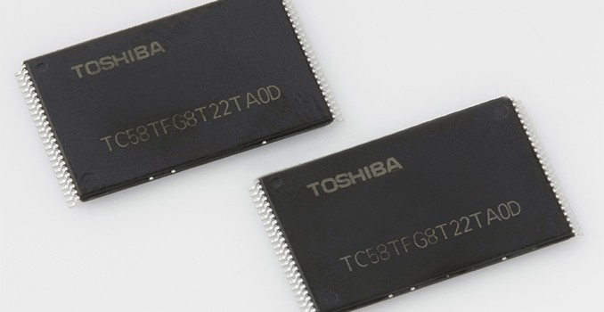
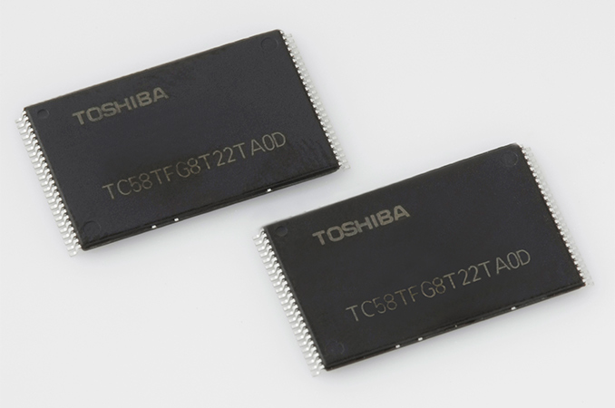
Note: Images are for illustrative purposes only.

Related Reading: