SOC


Gen-Z Consortium Formed: Developing a New Memory Interconnect

Gen-Z Consortium Formed: Developing a New Memory Interconnect

Anyone tasked with handling the way data is moved around a processor deserves praise. It takes time, dedication and skill to design something that not only works appropriately and for all edge cases, but also can run at speed and seamlessly for softwa…

Gen-Z Consortium Formed: Developing a New Memory Interconnect

Gen-Z Consortium Formed: Developing a New Memory Interconnect

Anyone tasked with handling the way data is moved around a processor deserves praise. It takes time, dedication and skill to design something that not only works appropriately and for all edge cases, but also can run at speed and seamlessly for softwa…

NVIDIA Teases Xavier, a High-Performance ARM SoC for Drive PX & AI

NVIDIA Teases Xavier, a High-Performance ARM SoC for Drive PX & AI

Ever since NVIDIA bowed out of the highly competitive (and high pressure) market for mobile ARM SoCs, there has been quite a bit of speculation over what would happen with NVIDIA’s SoC business. With the company enjoying a good degree of success with projects like the Drive system and Jetson, signs have pointed towards NVIDIA continuing their SoC efforts. But in what direction they would go remained a mystery, as the public roadmap ended with the current-generation Parker SoC. However we finally have an answer to that, and the answer is Xavier.

At NVIDIA’s GTC Europe 2016 conference this morning, the company has teased just a bit of information on the next generation Tegra SoC, which the company is calling Xavier (ed: in keeping with comic book codenames, this is Professor Xavier of the X-Men). Details on the chip are light – the chip won’t even sample until over a year from now – but NVIDIA has laid out just enough information to make it clear that the Tegra group has left mobile behind for good, and now the company is focused on high performance SoCs for cars and other devices further up the power/performance spectrum.

NVIDIA ARM SoCs
  Xavier Parker Erista (Tegra X1)
CPU 8x NVIDIA Custom ARM 2x NVIDIA Denver +
4x ARM Cortex-A57
4x ARM Cortex-A57 +
4x ARM Cortex-A53
GPU Volta, 512 CUDA Cores Pascal, 256 CUDA Cores Maxwell, 256 CUDA Cores
Memory ? LPDDR4, 128-bit Bus LPDDR3, 64-bit Bus
Video Processing 7680×4320 Encode & Decode 3840x2160p60 Decode
3840x2160p60 Encode
3840x2160p60 Decode
3840x2160p30 Encode
Transistors 7B ? ?
Manufacturing Process TSMC 16nm FinFET+ TSMC 16nm FinFET+ TSMC 20nm Planar

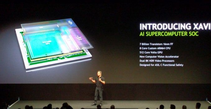
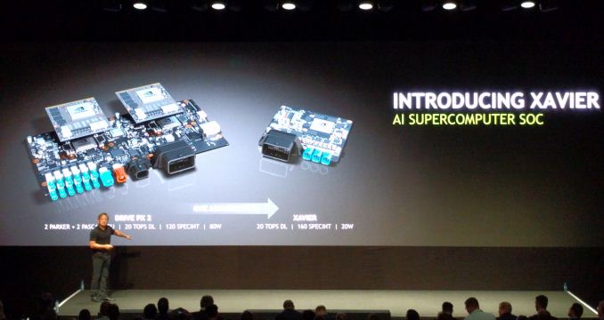
So what’s Xavier? In a nutshell, it’s the next generation of Tegra, done bigger and badder. NVIDIA is essentially aiming to capture much of the complete Drive PX 2 system’s computational power (2x SoC + 2x dGPU) on a single SoC. This SoC will have 7 billion transistors – about as many as a GP104 GPU – and will be built on TSMC’s 16nm FinFET+ process. (To put this in perspective, at GP104-like transistor density, we’d be looking at an SoC nearly 300mm2 big)

Under the hood NVIDIA has revealed just a bit of information of what to expect. The CPU will be composed of 8 custom ARM cores. The name “Denver” wasn’t used in this presentation, so at this point it’s anyone’s guess whether this is Denver 3 or another new design altogether. Meanwhile on the GPU side, we’ll be looking at a Volta-generation design with 512 CUDA Cores. Unfortunately we don’t know anything substantial about Volta at this time; the architecture was bumped further down NVIDIA’s previous roadmaps for Pascal, and as Pascal just launched in the last few months, NVIDIA hasn’t said anything further about it.

Meanwhile NVIDIA’s performance expectations for Xavier are significant. As mentioned before, the company wants to condense much of Drive PX 2 into a single chip.  With Xavier, NVIDIA wants to get to 20 Deep Learning Tera-Ops (DL TOPS), which is a metric for measuring 8-bit Integer operations. 20 DL TOPS happens to be what Drive PX 2 can hit, and about 43% of what NVIDIA’s flagship Tesla P40 can offer in a 250W card. And perhaps more surprising still, NVIDIA wants to do this all at 20W, or 1 DL TOPS-per-watt, which is one-quarter of the power consumption of Drive PX 2, a lofty goal given that this is based on the same 16nm process as Pascal and all of the Drive PX 2’s various processors.

NVIDIA’s envisioned application for Xavier, as you might expect, is focused on further ramping up their automotive business. They are pitching Xavier as an “AI Supercomputer” in relation to its planned high INT8 performance, which in turn is a key component of fast neural network inferencing. What NVIDIA is essentially proposing then is a beast of an inference processor, one that unlike their Tesla discrete GPUs can function on a stand-alone basis. Coupled with this will be some new computer vision hardware to feed Xavier, including a pair of 8K video processors and what NVIDIA is calling a “new computer vision accelerator.”

Wrapping things up, as we mentioned before, Xavier is a far future product for NVIDIA. While the company is teasing it today, the SoC won’t begin sampling until Q4 of 2017, and that in turn implies that volume shipments won’t even be until 2018. But with that said, with their new focus on the automotive market, NVIDIA has shifted from an industry of agile competitors and cut-throat competition, to one where their customers would like as much of a heads up as possible. So these kinds of early announcements are likely going to become par for the course for NVIDIA.

NVIDIA Teases Xavier, a High-Performance ARM SoC for Drive PX & AI

NVIDIA Teases Xavier, a High-Performance ARM SoC for Drive PX & AI

Ever since NVIDIA bowed out of the highly competitive (and high pressure) market for mobile ARM SoCs, there has been quite a bit of speculation over what would happen with NVIDIA’s SoC business. With the company enjoying a good degree of success with projects like the Drive system and Jetson, signs have pointed towards NVIDIA continuing their SoC efforts. But in what direction they would go remained a mystery, as the public roadmap ended with the current-generation Parker SoC. However we finally have an answer to that, and the answer is Xavier.

At NVIDIA’s GTC Europe 2016 conference this morning, the company has teased just a bit of information on the next generation Tegra SoC, which the company is calling Xavier (ed: in keeping with comic book codenames, this is Professor Xavier of the X-Men). Details on the chip are light – the chip won’t even sample until over a year from now – but NVIDIA has laid out just enough information to make it clear that the Tegra group has left mobile behind for good, and now the company is focused on high performance SoCs for cars and other devices further up the power/performance spectrum.

NVIDIA ARM SoCs
  Xavier Parker Erista (Tegra X1)
CPU 8x NVIDIA Custom ARM 2x NVIDIA Denver +
4x ARM Cortex-A57
4x ARM Cortex-A57 +
4x ARM Cortex-A53
GPU Volta, 512 CUDA Cores Pascal, 256 CUDA Cores Maxwell, 256 CUDA Cores
Memory ? LPDDR4, 128-bit Bus LPDDR3, 64-bit Bus
Video Processing 7680×4320 Encode & Decode 3840x2160p60 Decode
3840x2160p60 Encode
3840x2160p60 Decode
3840x2160p30 Encode
Transistors 7B ? ?
Manufacturing Process TSMC 16nm FinFET+ TSMC 16nm FinFET+ TSMC 20nm Planar

So what’s Xavier? In a nutshell, it’s the next generation of Tegra, done bigger and badder. NVIDIA is essentially aiming to capture much of the complete Drive PX 2 system’s computational power (2x SoC + 2x dGPU) on a single SoC. This SoC will have 7 billion transistors – about as many as a GP104 GPU – and will be built on TSMC’s 16nm FinFET+ process. (To put this in perspective, at GP104-like transistor density, we’d be looking at an SoC nearly 300mm2 big)

Under the hood NVIDIA has revealed just a bit of information of what to expect. The CPU will be composed of 8 custom ARM cores. The name “Denver” wasn’t used in this presentation, so at this point it’s anyone’s guess whether this is Denver 3 or another new design altogether. Meanwhile on the GPU side, we’ll be looking at a Volta-generation design with 512 CUDA Cores. Unfortunately we don’t know anything substantial about Volta at this time; the architecture was bumped further down NVIDIA’s previous roadmaps for Pascal, and as Pascal just launched in the last few months, NVIDIA hasn’t said anything further about it.

Meanwhile NVIDIA’s performance expectations for Xavier are significant. As mentioned before, the company wants to condense much of Drive PX 2 into a single chip.  With Xavier, NVIDIA wants to get to 20 Deep Learning Tera-Ops (DL TOPS), which is a metric for measuring 8-bit Integer operations. 20 DL TOPS happens to be what Drive PX 2 can hit, and about 43% of what NVIDIA’s flagship Tesla P40 can offer in a 250W card. And perhaps more surprising still, NVIDIA wants to do this all at 20W, or 1 DL TOPS-per-watt, which is one-quarter of the power consumption of Drive PX 2, a lofty goal given that this is based on the same 16nm process as Pascal and all of the Drive PX 2’s various processors.

NVIDIA’s envisioned application for Xavier, as you might expect, is focused on further ramping up their automotive business. They are pitching Xavier as an “AI Supercomputer” in relation to its planned high INT8 performance, which in turn is a key component of fast neural network inferencing. What NVIDIA is essentially proposing then is a beast of an inference processor, one that unlike their Tesla discrete GPUs can function on a stand-alone basis. Coupled with this will be some new computer vision hardware to feed Xavier, including a pair of 8K video processors and what NVIDIA is calling a “new computer vision accelerator.”

Wrapping things up, as we mentioned before, Xavier is a far future product for NVIDIA. While the company is teasing it today, the SoC won’t begin sampling until Q4 of 2017, and that in turn implies that volume shipments won’t even be until 2018. But with that said, with their new focus on the automotive market, NVIDIA has shifted from an industry of agile competitors and cut-throat competition, to one where their customers would like as much of a heads up as possible. So these kinds of early announcements are likely going to become par for the course for NVIDIA.

CEVA Launches Fifth-Generation Machine Learning Image and Vision DSP Solution: CEVA-XM6

CEVA Launches Fifth-Generation Machine Learning Image and Vision DSP Solution: CEVA-XM6

Deep learning, neural networks and image/vision processing is already a large field, however many of the applications that rely on it are still in their infancy. Automotive is the prime example that uses all of these areas, and solutions to the automotive ‘problem’ are require significant understanding and development in both hardware and software – the ability to process data with high accuracy in real-time opens up a number of doors for other machine learning codes, and all that comes afterwards is cost and power. The CEVA-XM4 DSP was aimed at being the first programmable DSP to support deep learning, and the new XM6 IP (along with the software ecosystem) is being launched today under the heading of stronger efficiency, compute, and new patents regarding power saving features.

Playing the IP Game

When CEVA launched the XM4 DSP, with the ability to infer pre-trained algorithms in fixed-point math to a similar (~1%) accuracy as the full algorithms, it won a number of awards from analysts in the field, claiming high performance and power efficiency over competing solutions and the initial progression for a software framework. The IP announcement was back in Q1 2015, with licensees coming on board over the next year and the first production silicon using the IP rolling off the line this year. Since then, CEVA has announced its CDNN2 platform, a one-button compilation tool for trained networks to be converted into suitable code for CEVA’s XM IPs. The new XM6 integrates the previous XM4 features, with improved configurations, access to hardware accelerators, new hardware accelerators, and still retains compatibility with the CDNN2 platform such that code suitable for XM4 can be run on XM6 with improved performance.

CEVA is in the IP business, like ARM, and works with semiconductor licensees that then sell to OEMs. This typically results in a long time-to-market, especially when industries such as security and automotive are moving at a rapid pace. CEVA is promoting the XM6 as a scalable, programmable DSP that can scale across markets with a single code base, while also using additional features to improve power, cost and performance.

The announcement today covers the new XM6 DSP, CEVA’s new set of imaging and vision software libraries, a set of new hardware accelerators and integration into the CDNN2 ecosystem. CDNN2 is a one-button compilation tool, detecting convolution and applying the best methodology for data transfer over the logic blocks and accelerators.

XM6 will support OpenCL and C++ development tools, and the software elements include CEVA’s computer vision, neural network and vision processing libraries with third-party tools as well. The hardware implements an AXI interconnect for the processing parts of the standard XM6 core to interact with the accelerators and memory. Along with the XM6 IP, there are hardware accelerators for convolution (CDNN assistance) allowing lower power fixed function hardware to cope with difficult parts of neural network systems such as GoogleNet, De-Warp for adjusting images taken on fish-eye or distorted lenses (once the distortion of an image is known, the math for the transform is fixed-function friendly), as well as other third party hardware accelerators.

The XM6 promotes two new specific hardware features that will aid the majority of image processing and machine learning algorithms. The first is scatter-gather, or the ability to read values from 32 addresses in L1 cache into vector registers in a single cycle. The CDNN2 compilation tool identifies serial code loading and implements vectorization to allow this feature, and scatter-gather improves data loading time when the data required is distributed through the memory structure. As the XM6 is configurable IP, the size/associativity of the L1 data store is adjustable at the silicon design level, and CEVA has stated that this feature will work with any size L1. The vector registers for processing at this level are 8-wide VLIW implementations, meaning ‘feed the beast’ is even more important than usual.

The second feature is called ‘sliding-window’ data processing, and this specific technique for vision processing has been patented by CEVA. There are many ways to process an image for either processing or intelligence, and typically an algorithm will use a block or tile of pixels at once to perform what it needs to. For the intelligence part, a number of these blocks will overlap, resulting in areas of the image being reused at different parts of the computation. CEVA’s method is to retain that data, resulting in fewer bits being needed in the next step of analysis. If this sounds straightforward (I was doing something similar with 3D differential equation analysis back in 2009), it is, and I was surprised that it had not been implemented in vision/image processing before. Reusing old data (assuming you have somewhere to store it) saves time and saves energy.

CEVA is claiming up to a 3x performance gain in heavy vector workloads for XM6 over XM4, with an average of 2x improvement for like-for-like ported kernels. The XM6 is also more configurable than the XM4 from a code perspective, offering ‘50% more control’.

With the specific CDNN hardware accelerator (HWA), CEVA cites that convolution layers in ecosystems such as GoogleNet consume the majority of cycles. The CDNN HWA takes this code and implements fixed hardware for it with 512 MACs using 16-bit support for up to an 8x performance gain (and 95% utilization). CEVA mentioned that a 12-bit implementation would save die area and cost for a minimal reduction in accuracy, however there are a number of developers requesting full 16-bit support for future projects, hence the choice.

Two of the big competitors for CEVA in this space, for automotive image/visual processing, is MobilEye and NVIDIA, with the latter promoting the TX1 for both training and inference for neural networks. Based on TX1 on a TSMC 20nm Planar process at 690 MHz, CEVA states that their internal simulations give a single XM6 based platform as 25x the efficiency and 4x the speed based on AlexNet and GoogleNet (with the XM6 also at 20nm, even though it will most likely be implemented at 16nm FinFET or 28nm). This would mean, extrapolating the single batch TX1 data published, that XM6 using AlexNet at FP16 can perform 268 images a second compared to 67, at around 800 mW compared to 5.1W. At 16FF, this power number is likely to be significantly lower (CEVA told us that their internal metrics were initially done at 28nm/16FF, but were redone on 20nm for an apples-to-apples with the TX1). It should be noted that TX1 numbers were provided for multi-batch which offered better efficiency over single batch, however other comparison numbers were not provided. CEVA also implements power gating with a DVFS scheme that allows low power modes when various parts of the DSP or accelerators are idle.

Obviously the advantage that NVIDIA has with their solution is availability and CUDA/OpenCL software development, both of which CEVA is attempting to address with one-button software platforms like CDNN2 and improved hardware such as XM6. It will be interesting to see which semiconductor partners and future implementations will combine this image processing with machine learning in the future. CEVA states that smartphones, automotive, security and commercial (drones, automation) applications are prime targets.