Smartphones


Samsung Announces Exynos 8890 with Cat.12/13 Modem and Custom CPU

Samsung Announces Exynos 8890 with Cat.12/13 Modem and Custom CPU

In an unexpected and surprise annoucement, Samsung today revealed its new generation flagship SoC – the Exynos 8. The Exynos 8890 to be more specific, is the successor to the Exynos 7420 that we’ve come to know very well in this year’s Galaxy flagships such as the Galaxy S6 or the Note5.

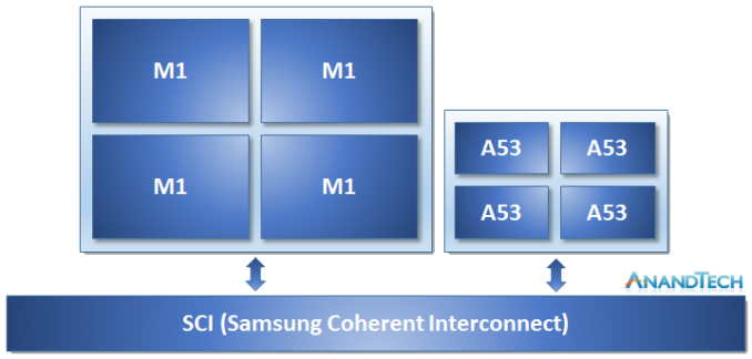
The Exynos 8890 is still an 4+4 big.LITTLE design using four Cortex A53 cores in the little cluster, but on the big cluster we see for the first time Samsung’s own custom developed CPU architecture deployed in silicon. The new core, officially called the Exynos M1, is the first fruit of years-long efforts by Samsung’s Austin R&D Center to try to create an in-house CPU architecture. What we do know of the M1 is that it’s still very similar to ARM’s big core architectures (And thus might be a derivative) such as the A72: It’s still a 3-wide OoO design with the same amount of execution pipelines and similar, although not quite identical pipeline stages on the execution units.

Samsung is claiming the Exynos 8890 will provide up to 30% higher performance and 10% better power efficiency than the Exynos 7420’s – although the wording is a bit vague and doesn’t specify if we’re talking about a pure architectural comparison or actual implementation comparison, as previous PR numbers on the Exynos 7420 also didn’t quite represent the full improvements of the chipset.

Samsung follows MediaTek’s example by dropping the use of ARM’s CCI IP in favour of designing their own cache-coherent interconnect fabric aptly named SCI (Samsung Coherent Interconnect). It seems that vendors are keen to try to improve their SoC architectures by designing fully optimized SoC fabric solutions and I guess Samsung saw the need to differentiate in this regard.

On the GPU side, we see usage of an ARM Mali T880MP12. This is the biggest Mali core implementation to date and increases the number of cores by 50% compared to the Exynos 7420’s MP8 configuration. Keeping in mind that the T880 also increases ALU pipelines per core by 50%, we’re looking at a 2.25x increase in computational power assuming Samsung kept the clock frequencies equal. Alternatively, they could go lower in frequency for much improved power efficiency. Samsung advertises 4K as an option for this SoC so likely we’re looking at a very powerful GPU setup.

Lastly, but not least, is the announcement that the Exynos 8890 is part of Samsung’s ModAP lineup, meaning this is a part with a modem. The new modem supports LTE Category 12 download speeds with up to 3x carrier aggregation up to 600Mbps or uploads speeds up to 150Mbps on Cat. 13 with CA. This effectively makes the new Shannon modem on the 8890 equal Qualcomm’s Snapdragon 820 modem capabilities. Until further future confirmation on the matter, I fail to use the “integrated” word in regards to the modem due to Samsung’s new product page presenting a graphic representing the modem/AP in a way that seems strikingly similar to a SiP (System-in-Package) solution, as opposed to an on-die solution.

The Exynos 8890 is announced to enter mass production in late 2015. With just six weeks left in the calendar year this likely means we’re already seeing silicon being etched as we speak, just in time for Samsung’s new Galaxy flagship early next year.

ARM Announces New Cortex-A35 CPU - Ultra-High Efficiency For Wearables & More

ARM Announces New Cortex-A35 CPU – Ultra-High Efficiency For Wearables & More

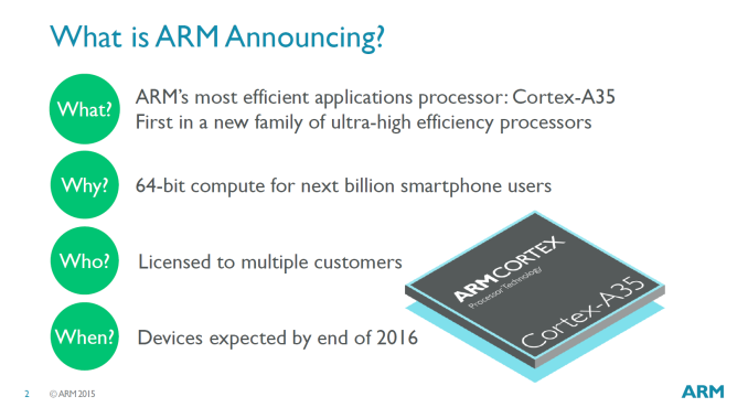
Today as part of the volley of announcements at ARM’s TechCon conference we discover ARM’s new low-power application-tier CPU architecture, the Cortex-A35. ARM follows an interesting product model: The company chooses to segment its IP offerings into different use-cases depending on market needs, designing different highly optimized architectures depending on the target performance and power requirements. As such, we see the Cortex-A lineup of application processors categorized in three groups: High performance, high efficiency, and ultra-high efficiency designs. In the first group we of course find ARM’s big cores such as the Cortex A57 or A72, followed by the A53 in more efficiency targeted use-cases or in tandem with big cores in big.LITTLE designs.
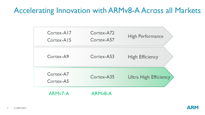
What seems to be counter-intuitive is that ARM sees the A35 not as a successor to the A53, but rather a replacement for the A7 and A5. During our in-depth analysis of the Cortex A53 in our Exynos 5433 review earlier this year I claimed that the A53 seemed to be more like an extension to the perf/W curve of the Cortex A7 instead of it being a part within the same power levels, and now with the A35 ARM seems to have validated this notion.

As such, the A35 is targeted at power targets below ~125mW where the Cortex A7 and A5 are still very commonly used. To give us an idea of what to expect from actual silicon, ARM shared with us a figure of 90mW at 1GHz on a 28nm manufacturing process. Of course the A35 will see a wide range of implementations on different process nodes such as for example 14/16nm or at much higher clock rates above 2GHz, similar to how we’ve come to see a wide range of process and frequency targets for the A53 today.

Most importantly, the A35 now completes ARM’s ARMv8 processor portfolio with designs covering the full range of power and efficiency targets. The A35 can also be used in conjunction with A72/A57/A53 cores in big.LITTLE systems, enabling for some very exotic configurations (A true tri-cluster comes to mind) depending if vendors see justification in implementing such SoCs.
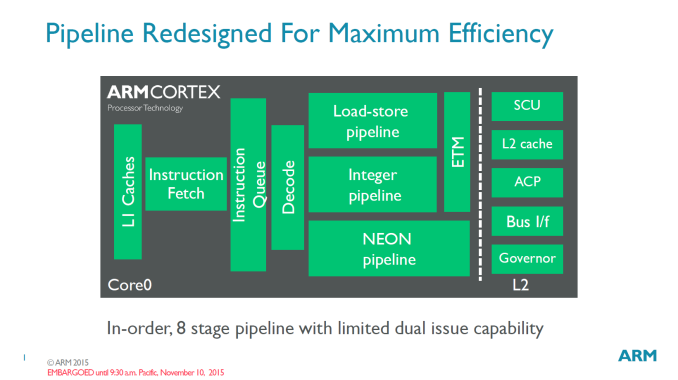
At heart, the A35 is still an in-order limited dual-issue architecture much like the A7 or A53. The 8-stage pipeline depth also hasn’t changed so from this high-level perspective we don’t see much difference in comparison to preceding designs. What ARM has done though is to improve the individual blocks for better performance and efficiency by having bits and pieces of architectural enhancements that are even newer than what big cores such as the A72 currently employ.
 
Areas where the A35 had focused attention on are front-end efficiency improvements, such as a redesigned instruction fetch unit that improves branch prediction. The instruction fetch bandwidth was balanced for power efficiency while the instruction queue is now smaller and also tuned for efficiency
 
It’s especially on memory benchmarks where the A35 will shine compared to the A7: The A35 adopts a lot of the Cortex A53’s memory architecture. On the L1 memory system of which A35 can have configurable 8 to 64KB of instruction and data caches we now see use of multi-stream automatic data prefetching and automatic write stream detection. The L2 memory system (configurable from 128KB to 1MB) has seen increased buffering capacity and resource sharing while improving write stream efficiency and introducting coherency optimizations to reduce contention.
 
The NEON/FP pipeline has seen the biggest advancements, besides improved store performance the new units now add fully pipelined double precision multiply capability. The pipeline has also seen improvements in terms of area efficiency, part of the reason enabling the A35 to be smaller than the A53.
 
In terms of power management, the A35 much like the A53 now implements hardware retention states for both the main CPU core and NEON pipeline (separate power domains). What seems to be interesting here is that there is now a hardware governor within the CPU cluster able to arbitrate automatic entry and exit for retention states. Until now we’ve seen very little to no use of retention states by vendors, the only SoC that I’ve confirmed to use it was the Snapdragon 810 and that was subsequently disabled in later software updates in favour of just using the core power collapse CPU idle state.
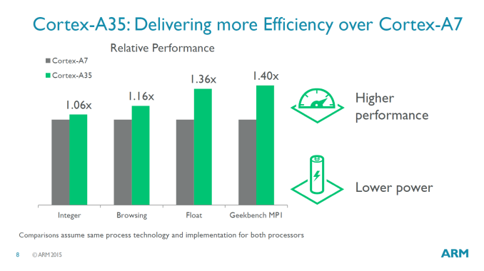
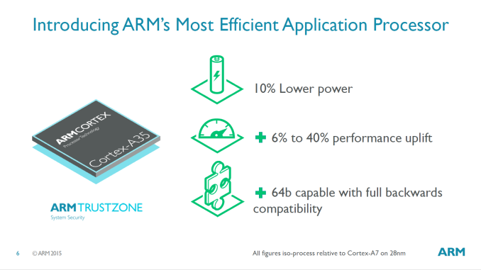
At the same frequency and process, the A35 architecture (codenamed Mercury), promises to be 10% lower power than the A7 while giving an 6-40% performance uplift depending on use-case. In integer workloads (SPECint2006) the A35 gives about 6% higher throughput than the A7, while floating point (SPECfp2000) is supposed to give a more substantial 36% increase.

What is probably more interesting are apples-to-apples performance and power comparisons to the A53. Here the A35 actually is extremely intriguing as it is able to match the A53’s performance from 80% to up to 100% depending on use-case. Browser workloads are where the A35 will trail behind the most and only be able to provide around 80% of the A53’s performance. Integer workloads are quoted at coming in at 84-85% of the Apollo core, while as mentioned earlier, memory-heavy workloads are supposed to be on par with the larger bretheren.
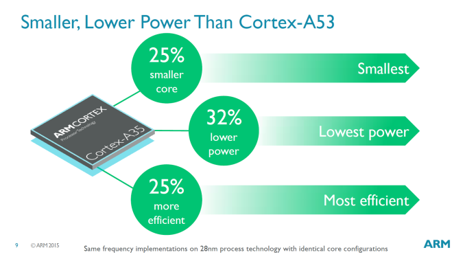
What puts things in perspective though is that the A35 is able to achieve all of this at 75% the core size and 68% the power of the A53. ARM claims that the A35 and A53 may still be used side-by-side and even envisions big.LITTLE A53.A35 designs, but I have a hard time justifying continued usage of the A53 because of the cost incentive for vendors to migrate over to the A35. Even in big.LITTLE with A72 big cores I find it somewhat hard to see why a vendor would choose to continue to use an A53 little cluster while they could theoretically just use a higher clocked A35 to compensate for the performance deficit. Even in the worst-case scenario where the power advantage would be eliminated by running a higher frequency, vendors would still be able to gain from the switch due to the smaller core and subsequent reduced die size.
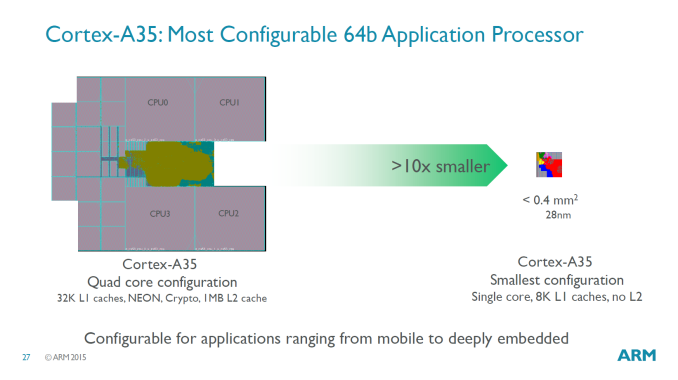
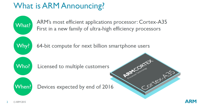
The A35 is touted as ARM’s most configurable processor with vendors able to alter their designs far beyond simple choices such the core-count within a cluster. Designers will now also be able to choose whether they want NEON, Crypto, ACP or even the L2 blocks included in their implementations. The company envisions this to be processor for the next billion smartphone users and we’ll likely see it in a very large variety of SoCs powering IoT devices such as wearables and embedded platforms, to budget smartphones and even high-end ones in big.LITTLE configurations.

ARM expects first devices with the A35 to ship by the end of 2016. Due to the sheer number of possible applications and expected volume, the Cortex A35 will undoubtedly be a very important CPU core for ARM that will be with us for quite some time to come. 

Google Begins Offline Maps Rollout on Android

Google Begins Offline Maps Rollout on Android

Earlier this year at Google I/O it was announced that Google Maps for Android and iOS would be receiving an update that would add the ability to save maps for offline viewing. Interestingly enough, this feature has actually existed and been removed from Google Maps on more than one occasion, and so such a prominent announcement gave some hope that it would stick around for good this time. Today the update is finally rolling out to Maps users on Android.

The feature works in a fairly straightforward manner. When searching a location in maps there will now be a download button in the information page about that location. You can then scroll around to fit the parts of the map you need into the box shown on screen, and when you name and save it the maps for that area will be permanently stored on your device. The applications for this feature are fairly obvious, such as storing maps of areas where you won’t have a cell signal, or of places you’ll be travelling to in other countries where your phone won’t work.

The new version of Google Maps with offline maps is rolling out now on Android, and an updated version for iOS will be coming in the near future.

Google Begins Offline Maps Rollout on Android

Google Begins Offline Maps Rollout on Android

Earlier this year at Google I/O it was announced that Google Maps for Android and iOS would be receiving an update that would add the ability to save maps for offline viewing. Interestingly enough, this feature has actually existed and been removed from Google Maps on more than one occasion, and so such a prominent announcement gave some hope that it would stick around for good this time. Today the update is finally rolling out to Maps users on Android.

The feature works in a fairly straightforward manner. When searching a location in maps there will now be a download button in the information page about that location. You can then scroll around to fit the parts of the map you need into the box shown on screen, and when you name and save it the maps for that area will be permanently stored on your device. The applications for this feature are fairly obvious, such as storing maps of areas where you won’t have a cell signal, or of places you’ll be travelling to in other countries where your phone won’t work.

The new version of Google Maps with offline maps is rolling out now on Android, and an updated version for iOS will be coming in the near future.