Smartphones


Chinese Tech Giant LeEco Enters US Market with Le Pro3 and Le S3 Smartphones, Range of UHD TVs

Chinese Tech Giant LeEco Enters US Market with Le Pro3 and Le S3 Smartphones, Range of UHD TVs

LeEco announced its official entry into the U.S. market at its “Ignite the Eco World” event in San Francisco, an important step in the company’s globalization plan. Its initial products include two large-screen smartphones, a range of 4K TVs, and new content partnerships.

LeEco may be the biggest tech company you’ve never heard of. The Chinese company began life as LeTV in 2004 as a streaming content provider and is often referred to as the “Netflix of China.” It then began creating its own movie and TV content with its Le Vision Pictures studio and then expanded into hardware, selling TVs that plugged into its streaming service. More recently, it has expanded its hardware lineup to include smartphones and even a connected bicycle and electric car. It even has its own Uber-like taxi service in China, Yidao.

LeEco now looks to extend its reach further west. Earlier this year it purchased U.S.-based TV maker Vizio, the second largest brand in the U.S., for $2 billion, giving it a familiar name and a foothold in a market wary of Chinese brands. LeEco also purchased Dichotomy Creative Group in September, rebranding it Le Vision Entertainment. The new division is headquartered in Los Angeles and will be responsible for creating original English-language content spanning movies, TV, VR, and the Web. LeEco is even setting up its global headquarters in Silicon Valley (its campus in Beijing will remain its headquarters for China), having purchased a 48-acre plot of land in San Jose, California from Yahoo that will eventually employ some 12,000 people.

LeEco’s US Ecophone Lineup
  Le Pro3 Le S3
SoC Qualcomm Snapdragon 821
(MSM8996 Pro)

2x Kryo @ 2.34GHz
2x Kryo @ 2.19GHz
Adreno 530 @ 653MHz

Qualcomm Snapdragon 652
(MSM8976)

4x Cortex-A72 @ 1.80GHz
4x Cortex-A53 @ 1.44GHz
Adreno 510

Display 5.5-inch 1920×1080 IPS LCD 5.5-inch 1920×1080 IPS LCD
Dimensions 151.4 x 73.9 x 7.5 mm
177 grams
151.1 x 74.2 x 7.5 mm
153 grams
RAM 4GB LPDDR4 3GB LPDDR3-1866
NAND 64GB 32GB (eMMC 5.1)
Battery 4070 mAh
non-replaceable
Qualcomm Quick Charge 3.0
3000 mAh
non-replaceable
Qualcomm Quick Charge 3.0
Front Camera 8MP, 1.4µm pixels, f/2.2 8MP, 1.4µm pixels, f/2.2
Rear Camera 16MP, f/2.0, PDAF, dual-tone LED flash 16MP, f/2.0, PDAF, HDR, dual-tone LED flash
Modem Qualcomm X12 LTE (Integrated)
2G / 3G / 4G LTE (Category 12/13)
Qualcomm X8 LTE (Integrated)
2G / 3G / 4G LTE (Category 7)
SIM Size NanoSIM 2x NanoSIM (dual standby)
Wireless 802.11a/b/g/n/ac, BT 4.2, NFC, IrLED, GPS/GNSS 802.11a/b/g/n/ac, BT 4.1, IrLED, GPS/GNSS
Connectivity USB 2.0 Type-C
Launch OS Android 6.0.1 with EUI 5.8
Launch Price $399 $249

To kickstart its U.S. strategy, LeEco is offering two smartphones: the Le Pro3 and the Le S3. Both phones have 5.5-inch 1080p displays, but use different internal hardware. The Le Pro3 includes Qualcomm’s latest Snapdragon 821 SoC, 4GB of LPDDR4 RAM, and 64GB of internal storage. Given its emphasis on streaming content it’s probably not too surprising it does not offer additional storage tiers or microSD card support. Its most interesting feature is a large 4070mAh battery, which should help keep the screen lit for extended movie watching.

The Le S3 comes with a Qualcomm Snapdragon 652 SoC, which combines four ARM Cortex-A72 CPU cores, four Cortex-A53 cores, and an Adreno 510 GPU that supports all of the latest 3D graphics APIs. We saw its smaller sibling, the Snapdragon 650 that comes with two fewer A72 cores, push the performance of Xiaomi’s Redmi Note 3 Pro to near flagship levels, so the Le S3 has good performance potential; however, in my brief time with the phone, I noticed some stuttering when navigating the UI and far too many instances where frame rate dropped below 60fps, more so than with the Redmi Note 3 Pro.

The Le S3 also comes with 3GB of LPDDR3 RAM, which should be adequate, but only 32GB of internal storage. For a device that needs to cache lots of music and videos, and still have room for pictures and apps, we definitely would like to see more NAND, especially without microSD card support. The Le S3 also does not get a big battery like the Pro3; its 3000mAh cell is a typical size for 5.1- to 5.2-inch phones rather than a 5.5-inch phablet.


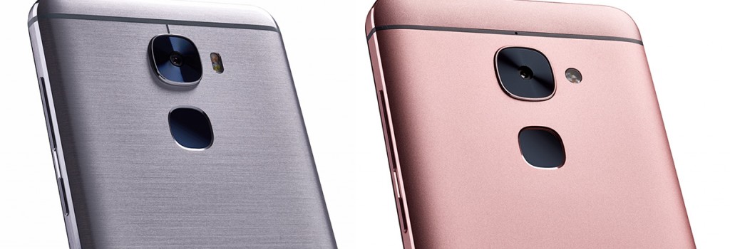
Le Pro3 (left), Le S3 (right)

Both phones have a similar camera setup, with an 8MP front-facing camera and a 16MP primary camera that has an f/2.0 lens and PDAF for faster focusing but does not include optical image stabilization (OIS). Video recording options are pretty basic, supporting only 2160p30 (4K), 1080p30, and 720p30 modes, and with no electronic image stabilization (EIS) option, videos can look pretty shaky.


Le S3 (rose gold)

LeEco eliminated the 3.5mm headphone jack from its phones before Apple axed the analog port in its iPhone 7, opting to pass audio over the USB Type-C port instead. Both the Le Pro3 and Le S3 support LeEco’s Continual Digital Lossless Audio (CDLA) technology that passes digital audio over USB. CDLA compatible earphones, included with both phones, have their own DAC and audio processor that’s supposed to reduce noise and improve channel separation relative to traditional analog audio from a 3.5mm jack. A Type-C to 3.5mm adapter is also included so you can use traditional headphones too.

Both phones also support Dolby Atmos surround-sound technology thanks to the Snapdragon SoCs, which produces more realistic positional audio and even accounts for an object’s vertical position in the soundfield as well.

The Le Pro3 and Le S3 both use aluminum unibody construction and share a similar design language. On the back of the phones we find horizontal plastic antenna lines at the top and bottom, with a large, not-quite-circular camera surround and fingerprint scanner. LeEco was the first company to use Qualcomm’s ultrasonic Sense ID fingerprint sensor, but these phones are using the more common capacitive variety. The most obvious visual difference between the phones is the finish applied to the aluminum: The Le Pro3 has a brushed finish while the Le S3 has a sandblasted finish.

The phones also look quite similar from the front, with relatively small upper and lower bezels and a symmetric layout. Hiding behind the lower bezel is a set of capacitive, backlit buttons. The LeEco logo replaces the standard home glyph on the Pro 3 and is flanked by the recents and back buttons of the left and right, respectively. The only other difference is that the Pro 3 uses 2.5D curved glass, while the S3’s edge-to-edge Corning Gorilla Glass 3 is flat all the way to the edge, giving it a sharper feeling in the hand.

One thing that’s immediately obvious as soon as you turn on either phone is the ridiculously large black bezel on all sides of the screen. The black area is significantly larger in person than LeEco’s press renderings show. I have not seen a border this large on a phone in some time, at least not on a phone that costs more than $200. For me, it’s large enough to be distracting and, in my opinion, it gives the phones a low-cost look.

Both phones include an infrared LED on the top edge for remote control duties, which fits in with LeEco’s philosophy of enabling its hardware to work together. Centered on the bottom edge is a USB 2.0 Type-C port flanked by two perforated grilles. On the Pro 3 they’re covering a pair of speakers, although, having both so close together and firing downward will diminish the stereo effect.

Switching our focus to software, we find that both phones are still running Android 6 Marshmallow with LeEco’s Ecosystem User Interface (EUI) 5.8 running on top. It’s disappointing that the phones will not ship with Android 7, but the demo models I handled were at least running recent security patches (either September or October). What’s unique about EUI are the included apps and built in support for accessing LeEco’s streaming content. Swiping to the left of the default home screen opens LeView, a list of suggestions for video content that learns from your viewing habits, somewhat analogous to HTC’s BlinkFeed or Flipboard for news. Tapping the Live icon opens a 3×3 grid of live video previews of content available for streaming. The Le app gives more comprehensive access to LeEco’s catalog of videos, TV episodes, and music.

It should be obvious by now that LeEco’s business strategy is more Amazon than Apple; it makes money from selling content and uses hardware as a delivery system. Because its revenue is not hardware-focused like with many of its competitors, it can sell its products at competitive prices, even at cost if necessary. LeEco’s ultimate goal is to create an internet-connected ecosystem encompassing hardware, software, and content that provides seamless access to all forms of digital entertainment. That’s no easy task, especially in the U.S. where many entrenched companies, including cable providers, movie studios, TV broadcasters, and internet companies provide similar services, albeit not always in a holistic way.

LeEco thinks it has the answer to this problem with its EcoPlatform that’s open to third-party content providers and hardware partners, essentially giving them access to LeEco’s content delivery system with its apps and LeCloud network that encompasses more than 750 CDN nodes. LeEco announced a number of launch partners at its event, including Lionsgate, Showtime, Esquire, the History Channel, and Metro-Goldwyn-Mayer to name just a few, and it mentioned that another major content partner will be announced on November 2.

To get the most from an ecosystem, whether it’s Apple’s or Google’s or Amazon’s, you need to fully buy in. This is especially true with LeEco, where signing up for Le EcoPass grants you access to 5TB of cloud storage, unlimited monthly movie viewing, extended warranties on LeEco hardware, and access to two EcoPass days (think Black Friday sales) at LeMall.com, its online storefront. It also offers the LeRewards program that grants further discounts on products.

Both the Le Pro3 and Le S3, along with LeEco’s other products, will be available for purchase on November 2 at LeMall.com. The Le Pro3 will cost $399 and the Le S3 will cost $249. There will be a $100 LeRewards discount available for both phones, which will drop the prices to $299 and $149, respectively. The Le Pro3 will be available in two colors—gray and gold—while the Le S3 will be available in three colors—gray, gold, and rose gold. Both phones will be unlocked and are compatible with GSM networks from AT&T, T-Mobile, MetroPCS, and Cricket Wireless.

Huawei announces the HiSilicon Kirin 960: 4xA73 + 4xA53, G71MP8, CDMA

Huawei announces the HiSilicon Kirin 960: 4xA73 + 4xA53, G71MP8, CDMA

Last year we had the opportunity to attend HiSilicon’s launch event of the Kirin 950. The 950 SoC was the first to employ ARM’s Cortex A72 in a smartphone, and the big.LITTLE 4×4 A72/A53 configuration of the 950 powered most of Huawei’s flagships for 2016. It also marked a significant jump both in performance as well as efficiency compared to previous Kirin chipsets. The CPU part especially made such a good impression in our review of the Mate 8, and at the time we estimated that it would easily trade blows with Qualcomm and Samsung’s own custom ARM microarchitecture designs, Kryo and Exynos M1, in their respective SoCs and flagship smartphones. Ultimately the Kirin 950 exceeded our expectations, in part due to the rather lackluster showing of this year’s custom-CPU powered Android devices.

The Kirin 950 was initially launched in the Huawei Mate 8, their new flagship smartphone. The SoC then followed into the Huawei P9, P9 Max, and the Honor 8 over the course of 2016 – essentially all the premium devices for Huawei and Huawei’s sub-brands, and contributing to the 106 million smartphone sales Huawei recorded in 2016 (30% of which were devices over $450). This is the success that Huawei wants to emulate with the Kirin 960.

Earlier this year, ARM announced their next generation microarchitecture IP in the form of the Cortex-A73 general-purpose core and the Mali-G71 graphics core. The A73 is a departure from the design of the A72 – the A72 was related to the A57 and A15 (Austin µarch family), whereas the A73 is a successor to the little-used Cortex A17 of the Sophia µarch family. Notable differences between the A73 to the A72 include a reduction of the decode-width from 3 to 2, but don’t let this change fool you as the new micro-architecture is supposed to be both faster and smaller (and efficient) than that of the A72. On the GPU side, the Mali G71 is an even bigger upgrade for ARM as it marks the first IP of the Bifrost architecture which brings beyond a nomenclature change from the Mali-Txxx series also significant performance and efficiency improvements.

Back in May we said that we would expect SoCs and devices with these new IPs by the end of the year, and indeed, the new Kirin 960 SoC from Huawei’s semiconductor subsidiary HiSilicon combines these two new technologies, promising the first commercial device to use them in due course.

While more details of the Kirin 960 will come forth over time as it makes its way into various devices, the official launch in Shanghai reiterated the partnership between HiSilicon and TSMC, using the new 16FFC process as the primary technology to enable the new SoC. As a reminder, the new process brings lower manufacturing cost thanks to lower mask count as well as better density due to new cell libraries.

HiSilicon High-End Kirin Lineup
SoC Kirin 950 Kirin 960
CPU 4x Cortex A72 (2.3 GHz)
4x Cortex A53 (1.8 GHz)
4x Cortex A73 (2.4 GHz)
4x Cortex A53 (1.8 GHz)
Memory
Controller
LPDDR3-933
or LPDDR4-1333
(hybrid controller)
LPDDR4-1800
GPU ARM Mali-T880MP4
900 MHz
ARM Mali-G71MP8
900 MHz
Interconnect ARM CCI-400 ARM CCI-550
Encode/
Decode
1080p H.264
Decode & Encode

2160p30 HEVC 
Decode

2160p30 HEVC & H.264
Decode & Encode

2160p60 HEVC
Decode

Camera/ISP Dual 14bit ISP
940MP/s
Improved
Dual 14bit ISP
Sensor Hub i5 i6
Storage eMMC 5.0 UFS 2.1
Integrated
Modem
Balong Integrated
UE Cat. 6 LTE
Integrated
UE Cat. 12 LTE
4x CA
4×4 MIMO

The Kirin 960 features the same 4×4 big.LITTLE design implementation as the Kirin 950, but using four Cortex A73 cores at 2.4 GHz (by contrast, the Cortex A72 cores in the 950 were at 2.3GHz, and 2.5 GHz in the Kirin 955). The little cores remain of the Cortex A53 micro-architecture and at the same 1.8 GHz configuration. 

Performance for the Kirin 960, as presented in Huawei’s announcement, is +10% single core performance and +18% on the multi-CPU performance compared to the Kirin 950. (This isn’t quite as much as we would have hoped from an A73 design, though.) HiSilicon presented GeekBench 4 scores for the new chipset and the K960 seems to benchmark around 2000 for single-core and 6400 for multi-core. The single-core scores slightly beat other Android SoCs in the market, however isn’t a too drastic improvement. We don’t have more exact sub-scores yet but one we know about is the vastly improved memory bandwidth of the new design that seems to beat all other SoCs at the moment. This is surely a result of both the Cortex A73’s strong memory subsystem as well as new use of the CCI-550 in the Kirin 950 that also promised an increase in effective memory bandwidth over the preceding CCI-400 design.

Initially we expected A73 designs to use the improved power envelope to drive up the clock frequencies higher, however in the case of the Kirin 960 the A73 is merely 100MHz above the Kirin 950 and actually 100MHz slower than the 955’s A72. The Kirin 950 already had the best sustainable CPU power envelope among this year’s SoCs so it would be surprising if HiSilicon decided to limit performance lower power even more, however we have confirmation that that is exactly what happened as we’ve been told the CPU’s power envelope has been lowered in favour of the GPU. This matches ARM’s philisophy about the new A73 that was presented back at TechDay, so the Kirin 960 seems to put this philosophy into practice. While there wasn’t talk about power efficiency we expect it to improve given that performance has gone up while power is supposed to have gone down.

A Bigger, Faster, More Powerful GPU

As mentioned earlier, the GPU sees a significant shift as we move from a Mali T880MP4 to a Mali-G71MP8, which essentially doubles the number of shader cores employed. HiSilicon decision to go with a wider GPU on the same process node was undoubtedly made much easier by the new G71’s much better die area efficiency. The new GPU runs at 900 MHz, the same as the older SoC. The combination of doubling the shader cores over the 950 and moving to a new architecture over the 950 results in a 180% increase in the GPU’s performance compared to the Kirin 950. As a result, Huawei is positioning the Kirin 960 directly above the other high-end SoCs launched this year (though we expect the other SoC vendors to also have respective increases with new generations soon). GFXBench Manhattan 3.0 and T-Rex Offscreen scores were showing the performance of the G71MP8 in above both the Snapdragon 820 and the Exynos 8890, but a tad under the new A10.

One of the popular criticisms of previous Huawei SoCs is the lack of graphics horsepower, with designs often opting for a four-core ‘MP4’ configuration despite using the high-performance graphics cores available from ARM. An MP4 configuration kept the die size of the SoC small and easier to implement. The downside of this is typically efficiency, suggesting that high graphics loads with fewer cores run at a worse point of the power efficiency curve to get an acceptable result.

Arguably most graphics scenarios on a smartphone, apart from extreme gaming titles and VR, can easily be provided by an MP4 configuration, and that was HiSilicon’s main rationale for past GPU configurations. However as Huawei devices mature and get more premium, there is also the fact that when buying a device above $450, the user should expect something performing near the best in the market, and it was clear that an MP4 design could not do that. The fact that the Kirin 960 moves to an MP8 design, while increasing die area and maximum power consumption, means that a Kirin SoC moves up to compete with larger GPU configurations such as Samsung’s large Mali designs in Exynos SoCs, Qualcomm’s Adreno in the Snapdragons, or the 6-cluster PowerVR GPU in Apple’s A-series. The mention of higher maximum power consumption comes with rather mixed feelings as the reasonably low GPU power was one of the aspects of the Kirin 950 that we especially praised when compared to other SoC designs, so we’ll have to wait to see real devices to see if this improvement isn’t a double-edged sword that introduces more severe GPU thermal throttling to the Kirin lineup.

Nevertheless, the improvement paves the way for things like VR, especially given Google’s recent announcement of Daydream VR (starting with the Snapdragon 821 in the Google Pixel smartphone). With the right software support and display, we would expect all future devices using the Kirin 960 to support Daydream VR. With API support, the Kirin 960 will be promoted with Vulkan.

New Category 12/13 Modem with a Custom CDMA Implementation

The Kirin 960 also features a new HiSilicon based modem, allowing up to LTE UE Category 12/13 connectivity for up to 600 Mbps transfers, equaling the specifications of Qualcomm’s Snapdragon 820 or Samsung’s Exynos 8890 modems. The modem is being promoted as the first commercial SoC to provide quad carrier aggregation to meet that speed, although it will obviously require carrier support in the region in order to do so. The modem supports 4×4 MIMO (at only 2xCA) as well as up to 256QAM spatial stream modulation.

One of the more interesting announcements from the Kirin briefing was the implementation of CDMA in the modem. Currently three smartphone modem providers have CDMA solutions (Qualcomm in integrated and discrete modems, Intel with discrete, Mediatek with VIA-based integrated), and we spoke with HiSilicon to confirm that this is a brand new custom CDMA solution, rather than a licensed platform. The value of CDMA is mixed, although a required element with certain carriers in China and the US, such that Huawei can now offer devices with the Kirin 960 can compete. It should be pointed out that CDMA certification for the US via the FCC takes 18-24 months, and I was unable to confirm when the process was started, so we may have to wait another year for a US-focused CDMA devices.

We noticed that previous Kirin modem designs were made under the ‘Balong’ name, however the name is dropped for this model. We were told that Balong is an old brand, and it was being dropped at this performance level, although it is unclear if the modem in the Kirin 960 or future SoCs will be branded. This may be related to the fact that when asked about the presence of CEVA LTE IP in the modem similar to previous models, we were told that the LTE design in the new modem is a custom internal design without CEVA.

The multimedia capabilities of the new SoC have also seen a great improvement as we finally see 4K recording made possible. The new chipset supports 4K30 HEVC/H.265 decoding and encoding. The camera ISP is improved as well and brings new features natively supporting dual-sensor RGB/Monochrome configurations such as found on the Huawei P9 and Honor 8. Previously these had relied on an additional external ISP chipset to make use of the new monochrome sensor.

A Good Showing

Naturally we expect Huawei’s next generation flagships to implement the Kirin 960 and variants over the next few months, especially as we move more towards Mobile World Congress in February. Similarly, updates to Kirin such as clock speed increases (the 955 is +200 MHz over the 950) moving into the middle of next year, along with an Honor device or two as time goes on. Huawei still keeps its HiSilicon SoC portfolio purely in-house, such that other smartphone OEMs do not have access to it, and given Huawei’s current success in unit sales and revenue, we would expect the continue the status quo on this front.

As perhaps was to be expected, when we asked Huawei about competitor’s 10nm plans (especially in light of recent news), no official statement was made. It’s very hard to not try to theorise comparisons between the Kirin 960 and next year’s Exynos and Snapdragons, while the former does bring substantial improvements to the table, it’ll be a hard fight competing against the new generation. Given Huawei and HiSilicon’s semiconductor product cycles, we might expect to hear more when TSMC’s foundry business starts making more public noise about the availability of future nodes and silicon mass production (or even Intel, depending on relationships). We will probably have to tune in next year, perhaps at a similar time, and there may be more concrete news about chipset roadmaps.

We expect the first devices to use the Kirin 960 to come out shortly.

Further Reading

Andrei’s Analysis of the ARM Cortex-A73 ‘Artemis’ CPU Microarchitecture
Ryan’s Analysis of the ARM Mali-G71 ‘Bifrost’ GPU Architecture
The Huawei Mate 8 Review
The Honor 8 / Huawei P9 Review

Huawei announces the HiSilicon Kirin 960: 4xA73 + 4xA53, G71MP8, CDMA

Huawei announces the HiSilicon Kirin 960: 4xA73 + 4xA53, G71MP8, CDMA

Last year we had the opportunity to attend HiSilicon’s launch event of the Kirin 950. The 950 SoC was the first to employ ARM’s Cortex A72 in a smartphone, and the big.LITTLE 4×4 A72/A53 configuration of the 950 powered most of Huawei’s flagships for 2016. It also marked a significant jump both in performance as well as efficiency compared to previous Kirin chipsets. The CPU part especially made such a good impression in our review of the Mate 8, and at the time we estimated that it would easily trade blows with Qualcomm and Samsung’s own custom ARM microarchitecture designs, Kryo and Exynos M1, in their respective SoCs and flagship smartphones. Ultimately the Kirin 950 exceeded our expectations, in part due to the rather lackluster showing of this year’s custom-CPU powered Android devices.

The Kirin 950 was initially launched in the Huawei Mate 8, their new flagship smartphone. The SoC then followed into the Huawei P9, P9 Max, and the Honor 8 over the course of 2016 – essentially all the premium devices for Huawei and Huawei’s sub-brands, and contributing to the 106 million smartphone sales Huawei recorded in 2016 (30% of which were devices over $450). This is the success that Huawei wants to emulate with the Kirin 960.

Earlier this year, ARM announced their next generation microarchitecture IP in the form of the Cortex-A73 general-purpose core and the Mali-G71 graphics core. The A73 is a departure from the design of the A72 – the A72 was related to the A57 and A15 (Austin µarch family), whereas the A73 is a successor to the little-used Cortex A17 of the Sophia µarch family. Notable differences between the A73 to the A72 include a reduction of the decode-width from 3 to 2, but don’t let this change fool you as the new micro-architecture is supposed to be both faster and smaller (and efficient) than that of the A72. On the GPU side, the Mali G71 is an even bigger upgrade for ARM as it marks the first IP of the Bifrost architecture which brings beyond a nomenclature change from the Mali-Txxx series also significant performance and efficiency improvements.

Back in May we said that we would expect SoCs and devices with these new IPs by the end of the year, and indeed, the new Kirin 960 SoC from Huawei’s semiconductor subsidiary HiSilicon combines these two new technologies, promising the first commercial device to use them in due course.

While more details of the Kirin 960 will come forth over time as it makes its way into various devices, the official launch in Shanghai reiterated the partnership between HiSilicon and TSMC, using the new 16FFC process as the primary technology to enable the new SoC. As a reminder, the new process brings lower manufacturing cost thanks to lower mask count as well as better density due to new cell libraries.

HiSilicon High-End Kirin Lineup
SoC Kirin 950 Kirin 960
CPU 4x Cortex A72 (2.3 GHz)
4x Cortex A53 (1.8 GHz)
4x Cortex A73 (2.4 GHz)
4x Cortex A53 (1.8 GHz)
Memory
Controller
LPDDR3-933
or LPDDR4-1333
(hybrid controller)
LPDDR4-1800
GPU ARM Mali-T880MP4
900 MHz
ARM Mali-G71MP8
900 MHz
Interconnect ARM CCI-400 ARM CCI-550
Encode/
Decode
1080p H.264
Decode & Encode

2160p30 HEVC 
Decode

2160p30 HEVC & H.264
Decode & Encode

2160p60 HEVC
Decode

Camera/ISP Dual 14bit ISP
940MP/s
Improved
Dual 14bit ISP
Sensor Hub i5 i6
Storage eMMC 5.0 UFS 2.1
Integrated
Modem
Balong Integrated
UE Cat. 6 LTE
Integrated
UE Cat. 12 LTE
4x CA
4×4 MIMO

The Kirin 960 features the same 4×4 big.LITTLE design implementation as the Kirin 950, but using four Cortex A73 cores at 2.4 GHz (by contrast, the Cortex A72 cores in the 950 were at 2.3GHz, and 2.5 GHz in the Kirin 955). The little cores remain of the Cortex A53 micro-architecture and at the same 1.8 GHz configuration. 

Performance for the Kirin 960, as presented in Huawei’s announcement, is +10% single core performance and +18% on the multi-CPU performance compared to the Kirin 950. (This isn’t quite as much as we would have hoped from an A73 design, though.) HiSilicon presented GeekBench 4 scores for the new chipset and the K960 seems to benchmark around 2000 for single-core and 6400 for multi-core. The single-core scores slightly beat other Android SoCs in the market, however isn’t a too drastic improvement. We don’t have more exact sub-scores yet but one we know about is the vastly improved memory bandwidth of the new design that seems to beat all other SoCs at the moment. This is surely a result of both the Cortex A73’s strong memory subsystem as well as new use of the CCI-550 in the Kirin 950 that also promised an increase in effective memory bandwidth over the preceding CCI-400 design.

Initially we expected A73 designs to use the improved power envelope to drive up the clock frequencies higher, however in the case of the Kirin 960 the A73 is merely 100MHz above the Kirin 950 and actually 100MHz slower than the 955’s A72. The Kirin 950 already had the best sustainable CPU power envelope among this year’s SoCs so it would be surprising if HiSilicon decided to limit performance lower power even more, however we have confirmation that that is exactly what happened as we’ve been told the CPU’s power envelope has been lowered in favour of the GPU. This matches ARM’s philisophy about the new A73 that was presented back at TechDay, so the Kirin 960 seems to put this philosophy into practice. While there wasn’t talk about power efficiency we expect it to improve given that performance has gone up while power is supposed to have gone down.

A Bigger, Faster, More Powerful GPU

As mentioned earlier, the GPU sees a significant shift as we move from a Mali T880MP4 to a Mali-G71MP8, which essentially doubles the number of shader cores employed. HiSilicon decision to go with a wider GPU on the same process node was undoubtedly made much easier by the new G71’s much better die area efficiency. The new GPU runs at 900 MHz, the same as the older SoC. The combination of doubling the shader cores over the 950 and moving to a new architecture over the 950 results in a 180% increase in the GPU’s performance compared to the Kirin 950. As a result, Huawei is positioning the Kirin 960 directly above the other high-end SoCs launched this year (though we expect the other SoC vendors to also have respective increases with new generations soon). GFXBench Manhattan 3.0 and T-Rex Offscreen scores were showing the performance of the G71MP8 in above both the Snapdragon 820 and the Exynos 8890, but a tad under the new A10.

One of the popular criticisms of previous Huawei SoCs is the lack of graphics horsepower, with designs often opting for a four-core ‘MP4’ configuration despite using the high-performance graphics cores available from ARM. An MP4 configuration kept the die size of the SoC small and easier to implement. The downside of this is typically efficiency, suggesting that high graphics loads with fewer cores run at a worse point of the power efficiency curve to get an acceptable result.

Arguably most graphics scenarios on a smartphone, apart from extreme gaming titles and VR, can easily be provided by an MP4 configuration, and that was HiSilicon’s main rationale for past GPU configurations. However as Huawei devices mature and get more premium, there is also the fact that when buying a device above $450, the user should expect something performing near the best in the market, and it was clear that an MP4 design could not do that. The fact that the Kirin 960 moves to an MP8 design, while increasing die area and maximum power consumption, means that a Kirin SoC moves up to compete with larger GPU configurations such as Samsung’s large Mali designs in Exynos SoCs, Qualcomm’s Adreno in the Snapdragons, or the 6-cluster PowerVR GPU in Apple’s A-series. The mention of higher maximum power consumption comes with rather mixed feelings as the reasonably low GPU power was one of the aspects of the Kirin 950 that we especially praised when compared to other SoC designs, so we’ll have to wait to see real devices to see if this improvement isn’t a double-edged sword that introduces more severe GPU thermal throttling to the Kirin lineup.

Nevertheless, the improvement paves the way for things like VR, especially given Google’s recent announcement of Daydream VR (starting with the Snapdragon 821 in the Google Pixel smartphone). With the right software support and display, we would expect all future devices using the Kirin 960 to support Daydream VR. With API support, the Kirin 960 will be promoted with Vulkan.

New Category 12/13 Modem with a Custom CDMA Implementation

The Kirin 960 also features a new HiSilicon based modem, allowing up to LTE UE Category 12/13 connectivity for up to 600 Mbps transfers, equaling the specifications of Qualcomm’s Snapdragon 820 or Samsung’s Exynos 8890 modems. The modem is being promoted as the first commercial SoC to provide quad carrier aggregation to meet that speed, although it will obviously require carrier support in the region in order to do so. The modem supports 4×4 MIMO (at only 2xCA) as well as up to 256QAM spatial stream modulation.

One of the more interesting announcements from the Kirin briefing was the implementation of CDMA in the modem. Currently three smartphone modem providers have CDMA solutions (Qualcomm in integrated and discrete modems, Intel with discrete, Mediatek with VIA-based integrated), and we spoke with HiSilicon to confirm that this is a brand new custom CDMA solution, rather than a licensed platform. The value of CDMA is mixed, although a required element with certain carriers in China and the US, such that Huawei can now offer devices with the Kirin 960 can compete. It should be pointed out that CDMA certification for the US via the FCC takes 18-24 months, and I was unable to confirm when the process was started, so we may have to wait another year for a US-focused CDMA devices.

We noticed that previous Kirin modem designs were made under the ‘Balong’ name, however the name is dropped for this model. We were told that Balong is an old brand, and it was being dropped at this performance level, although it is unclear if the modem in the Kirin 960 or future SoCs will be branded. This may be related to the fact that when asked about the presence of CEVA LTE IP in the modem similar to previous models, we were told that the LTE design in the new modem is a custom internal design without CEVA.

The multimedia capabilities of the new SoC have also seen a great improvement as we finally see 4K recording made possible. The new chipset supports 4K30 HEVC/H.265 decoding and encoding. The camera ISP is improved as well and brings new features natively supporting dual-sensor RGB/Monochrome configurations such as found on the Huawei P9 and Honor 8. Previously these had relied on an additional external ISP chipset to make use of the new monochrome sensor.

A Good Showing

Naturally we expect Huawei’s next generation flagships to implement the Kirin 960 and variants over the next few months, especially as we move more towards Mobile World Congress in February. Similarly, updates to Kirin such as clock speed increases (the 955 is +200 MHz over the 950) moving into the middle of next year, along with an Honor device or two as time goes on. Huawei still keeps its HiSilicon SoC portfolio purely in-house, such that other smartphone OEMs do not have access to it, and given Huawei’s current success in unit sales and revenue, we would expect the continue the status quo on this front.

As perhaps was to be expected, when we asked Huawei about competitor’s 10nm plans (especially in light of recent news), no official statement was made. It’s very hard to not try to theorise comparisons between the Kirin 960 and next year’s Exynos and Snapdragons, while the former does bring substantial improvements to the table, it’ll be a hard fight competing against the new generation. Given Huawei and HiSilicon’s semiconductor product cycles, we might expect to hear more when TSMC’s foundry business starts making more public noise about the availability of future nodes and silicon mass production (or even Intel, depending on relationships). We will probably have to tune in next year, perhaps at a similar time, and there may be more concrete news about chipset roadmaps.

We expect the first devices to use the Kirin 960 to come out shortly.

Further Reading

Andrei’s Analysis of the ARM Cortex-A73 ‘Artemis’ CPU Microarchitecture
Ryan’s Analysis of the ARM Mali-G71 ‘Bifrost’ GPU Architecture
The Huawei Mate 8 Review
The Honor 8 / Huawei P9 Review