Semiconductors


GlobalFoundries to Expand Capacities, Build a Fab in China

GlobalFoundries to Expand Capacities, Build a Fab in China

GlobalFoundries has announced plans to expand manufacturing capacities for its leading edge and mainstream production technologies in the U.S., Germany and Singapore. After the upgrades of the fabs are completed, the total 300-mm output of the company will increase by approximately 20%. In addition, GlobalFoundries intends to build a new 300mm fab in Chengdu, China, in a partnership with local authorities. The latter will produce chips using 130/180 nm and FD-SOI manufacturing technologies.

GlobalFoundries’ Expansion Plans
  Process Technologies

current and planned

Current Capacity*

wafer starts per month

Planned Increase Target Capacity*

wafer starts per month

Target Timeframe
Fab 1
(Dresden, Germany)
32 nm SOI
28 nm
22FDX (FD-SOI)
12FDX (FD-SOI)
up to 80,000 +40% ~110,000 2020
Fab 7
(Singapore)
130 nm
65/55 nm
40 nm
RF-SOI
68,000 +35% for 40 nm Over 68,000 2017~2018
Fabs
(Singapore)
180 nm unknown +?% for 180 nm unknown 2017~2018
Fab 8
(New York, USA)
28 nm
14LPP
7 nm
up to 60,000 +20% for 14LPP Over 60,000 Early 2018
Chengdu Fab
(China)
180/130 nm
22FDX (FD-SOI)
Ph. 1: 20,000
Ph. 2: 65,000
P1+P2: 85,000
Ph. 1: 2018+
Ph. 2: 2019+
*Please note that actual wafer starts per month (WSPM) output of a fab depends on multiple factors, including process technologies used. As a result, all the WSPM capacity numbers are relative and may not reflect actual performance. Keep in mind, that as foundries and IDMs increase usage of multi-patterning techniques, their effective WSPM output drops as wafers spend more time in the cleanroom. Hence, to keep the wafer starts per month capacity, chipmakers need to add equipment (which may, or may not, involve physical expansion of the cleanroom space).

Fab 8 to Gain 20% 14LPP FinFET Capacity

GlobalFoundries operates 10 fabs worldwide with four of them processing 300 mm wafers. The company’s most advanced fab is the Fab 8 located in Luther Forest Technology Campus (Saratoga County, New York) where the chipmaker produces flagship processors for AMD and some other leading developers of chips. To keep the Fab 8 up-to-date, GlobalFoundries spends billions of dollars on development of new manufacturing technologies and production equipment. Back in September, the company already announced plans to invest several billion in new tools to produce ICs (integrated circuits) using its 7 nm fabrication process and this week GlobalFoundries said it would invest in the expansion of the Fab 8’s manufacturing capacity.

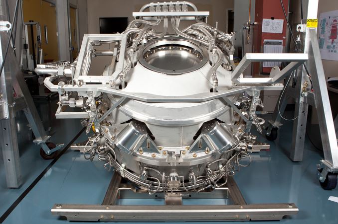
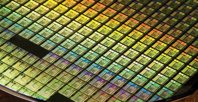
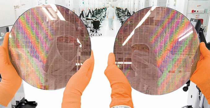
GlobalFoundries Fab 8. Photo by FinanceFeeds.net

After the latest expansion in 2013, the Fab 8’s capacity is around 60,000 wafer starts per month. The exact capacity today depends on several factors because the company now processes wafers using a more advanced process technology (the 14LPP) that uses multi-patterning, which effectively reduces capacity because each wafer spends more time in the cleanroom. In a bid to increase the output of 14LPP FinFET ICs by 20% by early 2018, the company intends to boost its production capacity. The firm said that the expansion does not involve physical expansion of the cleanroom, but the installation of additional more advanced step-and-scan systems and/or other tools into the existing space. For example, a switch from the TWINSCAN NXT:1960Bi to the TWINSCAN NXT:1980Di increases output of wafers by around 20% as the latter can process 275 wafers per hour versus 230 wafers per hour.

As the company is preparing to start high-volume manufacturing (HMV) of chips using its 7 nm FinFET technology in the second quarter of next year (so, several months ahead of the plan), the actual output of the Fab 8 remains to be seen. Initially, GlobalFoundries plans to use deep ultraviolet (DUV) lithography with quadruple patterning to produce chips using its 7 nm process, but sometime in 2019 it intends to start using extreme ultraviolet (EUV) lithography for a new wave of 7 nm designs. Usage of EUV will not eliminate multi-/quadruple-patterning, but will be used for cirical layers and will thus help to increase output of leading-edge chips. At present, the company does not talk about its 7 nm capacity, but it is logical to assume that the current expansion will have a positive effect on it as well.

In fact, the expansion of the Fab 8 is important for the fabless semiconductor industry as a whole because there are not a lot of foundries capable of producing ICs using FinFET manufacturing technologies. While numerous companies (like TowerJazz and Vanguard) ceased to develop leading-edge fabrication processes quite some time ago, SMIC and UMC are struggling with FinFETs as well. Moreover, neither of them are adopting FD-SOI-based planar technologies. As a result, there are only three pure-play foundries to offer HMV FinFETs to fabless chip designers: GlobalFoundries, Samsung Foundry and TSMC (Intel’s 10nm ARM Artisan IP foundry business is potentially to add to that list in due course). Besides, there are two companies to offer advanced FD-SOI-based planar technologies: GF and Samsung.

Fab 1 Gets More FD-SOI

Fab 1 used to be AMD’s flagship production facility and it remains GlobalFoundries’ highest-capacity plant that can process up to 80,000 wafers per month. While it does not produce chips using the most advanced technologies with FinFETs, it is used to make energy-efficient ICs using low-power and cost-optimized planar FD-SOI-based manufacturing processes. Since the development of FinFET-based chips costs significantly more than the development of ICs with planar transistors, planar process technologies continue to make sense for many designers of chips (especially smaller ones). To fulfill demand from such customers developing ICs for Internet of Things (IoT), smartphone, automotive electronic and other applications, GlobalFoundries plans to expand the capacity of the Fab 1 by 40% by 2020 (it is only going to expand the FD-SOI lines). GlobalFoundries did not elaborate whether the expansion involves the construction of new buildings, the physical increase of the cleanroom space of one (or both) of the two fab modules or installation of new equipment.

At present, the company offers a variety of planar manufacturing processes at Fab 1, including various 28 nm bulk technologies as well as its FD-SOI 22FDX (it uses back-end-of-line interconnect flow of STMicroelectronics’ 28nm FD-SOI, as well as front-end-of-line STM’s 14nm FD-SOI process technology). GlobalFoundries pins a lot of hopes on the FD-SOI technology and the significant expansion of the Fab 1 re-emphasizes this commitment.

The expansion of the factory will help to boost not only 22FDX output, but could also offer significant production capacities for developers designing for the next-gen FD-SOI technology, 12FDX (we do not say that all of the new equipment will be re-used for the 12FDX, but at least some tools will be). GlobalFoundries does not release too many details about the 12FDX process to the public, but it says that it enables “the performance of 10 nm FinFET with better power consumption and lower cost than 16nm FinFET,” while also offering a 15% geometry scaling benefit compared to “today’s FinFET technologies” (if by “today’s” GF means 14LPP and CLN16FF/FF+, then the 12FDX has a 15% higher transistor density compared to technologies based on 20 nm BEOLs). The company expects the first 12FDX tape-outs in the first half of 2019, so the expansion of the Fab 1 by 2020 will likely be a benefit for FD-SOI designers in general.

The First Fab in China

Meanwhile, GlobalFoundries’ FD-SOI efforts will not be limited to its Germany manufacturing facility (even though the Fab 1 will remain the key development site for the tech). The company’s first fab in China (which might be called the Fab 11, but we will call it the Chengdu fab for now) will also be able to produce chips using the 22FDX. But before jumping to the FD-SOI in China, let’s talk about the plant itself first.

The Chengdu fab will be built in a partnership between GlobalFoundries and the Chengdu municipality. The first phase of the fab will begin operations in 2018 and it will use mainstream 180/130 nm fabrication technologies. The fab will initially process around 20,000 wafers per month. It is important to note that the mainstream manufacturing technologies that the Chengdu fab will use were originally developed by Chartered and not by AMD for its CPUs. The second phase will start operations in 2019 and will eventually be able to process 65,000 wafers per month using the 22FDX technology.

When fully ramped, the Chengdu fab will have a capacity of approximately 1,000,000 wafers per year (so, around 83,000 ~ 85,000 wafers per month for the phase 1 and phase 2 when both are fully operational) and will be a tangible manufacturing asset for GlobalFoundries. The fab is meant to fulfill increasing demand from China-based developers of semiconductors, but it will also be used to make chips for other fabless companies using primarily the 22FDX process, further increasing FD-SOI manufacturing capacities of GlobalFoundries and making the tech more attractive to customers requiring very high product volumes.

It is noteworthy that one of the interested parties in GF’s 22FDX tech is Rockchip, which has so far used only bulk process technologies of TSMC, SMIC and GlobalFoundries to produce its mobile SoCs. Other adopters of FD-SOI are developers of various wireless chips (like modems) and ICs that have to be very energy-efficient (particularly in idle mode).

Singapore Fabs Get a Boost

Finally, in addition to expanding the leading edge Fab 1 and Fab 8 as well as building a new semiconductor manufacturing facility, GlobalFoundries intends to increase the output of its fabs in Singapore.

The company does not publish too many details about the Singapore expansion, but only says that it intends to increase 40 nm capacity at its 300-mm Fab 7 by 35% and also boost output of its lines processing wafers using its 180 nm manufacturing process. Furthermore, GlobalFoundries will install new tools to make chips using its RF-SOI fabrication tech presumably on 300 mm wafers (which may be a big deal).

The Right Capacity at the Right Time

Since modern fabs and production tools cost billions of dollars to build, semiconductor manufacturers typically cannot afford them standing idle. A lack of capacity means that foundries cannot land orders from customers and eventually lose market share to rivals. Therefore it is important to have the right capacity and process technologies at the right time.

According to IC Insights, sales of all pure-play foundries in 2016 totaled around $50 billion, growing 11% year-over-year. GlobalFoundries was the second largest contract maker of chips with an estimated $5.5 billion in revenue (keep in mind that the company does not officially comment on such numbers), up 10% YoY. In a bid to sustain growth, GlobalFoundries needs to gradually increase its production capacities and the installation of new tools will serve the purpose, just like building a new fab in China.

For foundries, expanding production capacities is a usual business and they always try to optimize their output to meet demands from customers. GlobalFoundries is selectively adding capacities to popular nodes (and companies like MediaTek, Qualcomm, and Rockchip have already welcomed the decision), which is a smart move. In addition, it plans to build a new fab in China, which is a clever way to address a particular territory.

Related Reading:

Samsung Foundry Announces 10nm SoC In Mass-Production

Samsung Foundry Announces 10nm SoC In Mass-Production

Today Samsung announced mass production of a SoC built on its third-generation 10nm “10LPE” manufacturing node. It was only this January that Samsung announced mass production of its 14LPP process that ended up being used in the Exynos 8890 and the Snapdragon 820 powering up a large amount of flagship devices this year.

This time around the announcement comes quite early compared to the past 2 years and I wasn’t expecting any news from the foundry till maybe later in the quarter. This does however bode well for the SoCs built on the process as they seem they’ll be able to easily make the spring 2017 device release schedule.

There wasn’t any specification as to what kind of SoC the mass production announcement is refering to, but it’s very likely we’re talking about S.LSI’s next generation Exynos – or maybe even Qualcomm’s Snapdragon 820 successor, both of which we’ll hopefully hear official announcements from in the coming months.

Samsung’s new 10nm FinFET process (10LPE) adopts an advanced 3D transistor structure with additional enhancements in both process technology and design enablement compared to its 14nm predecessor, allowing up to 30-percent increase in area efficiency with 27-percent higher performance or 40-percent lower power consumption. In order to overcome scaling limitations, cutting edge techniques such as triple-patterning to allow bi-directional routing are also used to retain design and routing flexibility from prior nodes.


Credit: DAC 2016 Samsung/Synopsys Breakfast – Ready to Design at 10nm!

The process promises some significant speed and power efficiency advantages over current generation designs so it’s likely the next generation of devices will see a large boost, similarly to how the first 14/16 SoCs had large improvements over previous generation 20/28nm designs.

Interestingly the new SoCs will have an edge on recent and upcoming designs still being released on 16nm manufacturing processes, such as Apple’s A10 or other TSMC customers who have to wait till next year for 10FF. This presents itself as an opportunity for vendors such as Samsung and Qualcomm to try to close the performance and efficiency gap seen in the current generation through the manufacturing process’ good timing.

Samsung Foundry Announces 10nm SoC In Mass-Production

Samsung Foundry Announces 10nm SoC In Mass-Production

Today Samsung announced mass production of a SoC built on its third-generation 10nm “10LPE” manufacturing node. It was only this January that Samsung announced mass production of its 14LPP process that ended up being used in the Exynos 8890 and the Snapdragon 820 powering up a large amount of flagship devices this year.

This time around the announcement comes quite early compared to the past 2 years and I wasn’t expecting any news from the foundry till maybe later in the quarter. This does however bode well for the SoCs built on the process as they seem they’ll be able to easily make the spring 2017 device release schedule.

There wasn’t any specification as to what kind of SoC the mass production announcement is refering to, but it’s very likely we’re talking about S.LSI’s next generation Exynos – or maybe even Qualcomm’s Snapdragon 820 successor, both of which we’ll hopefully hear official announcements from in the coming months.

Samsung’s new 10nm FinFET process (10LPE) adopts an advanced 3D transistor structure with additional enhancements in both process technology and design enablement compared to its 14nm predecessor, allowing up to 30-percent increase in area efficiency with 27-percent higher performance or 40-percent lower power consumption. In order to overcome scaling limitations, cutting edge techniques such as triple-patterning to allow bi-directional routing are also used to retain design and routing flexibility from prior nodes.


Credit: DAC 2016 Samsung/Synopsys Breakfast – Ready to Design at 10nm!

The process promises some significant speed and power efficiency advantages over current generation designs so it’s likely the next generation of devices will see a large boost, similarly to how the first 14/16 SoCs had large improvements over previous generation 20/28nm designs.

Interestingly the new SoCs will have an edge on recent and upcoming designs still being released on 16nm manufacturing processes, such as Apple’s A10 or other TSMC customers who have to wait till next year for 10FF. This presents itself as an opportunity for vendors such as Samsung and Qualcomm to try to close the performance and efficiency gap seen in the current generation through the manufacturing process’ good timing.

EUV Lithography Makes Good Progress, Still Not Ready for Prime Time

EUV Lithography Makes Good Progress, Still Not Ready for Prime Time

At the recent annual SPIE Advanced Lithography conference, Intel, TSMC and other leading semiconductor companies said that significant strides have been made in extreme ultraviolet lithography (EUVL) over the past year or so. Intel did not reveal when exactly it plans to start using EUV technology, but indicated that it will clearly utilize it once it is suitable for high-volume production of semiconductors and is sufficiently cost effective . Samsung and TSMC also intend to start inserting EUVL tools into production in the coming years.

Chip Production Gets Harder

As chipmakers transit to newer process technologies every several years, sizes of transistors and electronic circuits within microprocessors shrink, making them more complex and powerful, but also harder to manufacture using traditional photolithographic methods. Feature sizes of today’s circuits within modern chips can be as small as 42 nm, whereas modern semiconductor production tools use deep ultraviolet (DUV) argon fluoride (ArF) excimer lasers with 193 nm wavelength. To compensate for this difference, Intel and other makers of advanced chips use multiple techniques to enhance resolution of photolithographic equipment.

One of the key transistor density improving technologies is immersion lithography, which replaces the air gap between the lens and wafer with liquid, whose refraction index is higher than one. For example, purified deionized water has refraction index of 1.44 and this allows to enhance resolution of production tools by up to 40% depending on materials. Another key tech for contemporary semiconductor manufacturing is called multiple patterning, a semiconductor production technique that allows to increase feature density by resolving multiple lines on the same photoresist layer using multiple photomasks. Usage of multi-patterning essentially means that certain layers within one chip are exposed multiple times, which greatly increases complexity of manufacturing operations and stretches production cycles, essentially increasing costs of chips.

Intel has been using multi-patterning since mid-2000s and its 65 nm manufacturing technology. The technique did not cause a lot of troubles at first, but things got very complicated with the 14 nm fabrication process because the number of mask steps significantly increased compared to previous-gen technologies. Meanwhile it is taking the company longer to develop its 10 nm manufacturing process, tune its designs and achieve high yields than it used to be, which is why the company had to delay its Cannonlake CPUs from 2016 to 2017. It’s also important to note that Intel’s 14nm process introduced air gap dielectric in certain interconnect layers, which dramatically increased the number of engineering problems to overcome as introducing voids into the interconnect leads to structural instabilities that must be controlled appropriately.

Basically, as it becomes increasingly tougher to develop new manufacturing technologies and produce modern chips using currently available tools, the benefits of node-to-node transitions shrinks, which is rather dangerous for chipmakers from an economic standpoint. In order to address negative effects of multi-patterning, producers of step and scan systems used in semiconductor manufacturing significantly increased output of such tools, as well as enhanced their resolution and boosted their overlay and focus performance. For example, ASM Lithography (ASML), the world’s largest maker of scanners, claims that its latest TWINSCAN NXT:1980Di can process up to 275 wafers per hour and can be used to make chips using sub-10 nm process technologies. While such scanners will be utilized going forward, with so many mask steps required, a new method of photolithography will make far more sense.

EUV Makes a Big Promise, But Generates Big Challenges

EUV lithography, whose development started in 1985 and which used to be called Soft X-Ray, utilizes extreme ultraviolet wavelength of 13.5 nm. Using EUV can greatly enhance the feature density of chips without heavy reliance on multi-patterning and additional layers. For example, TSMC can produce 46 nm metal pitches with a single exposure, an operation that requires usage of four masks for an ArF scanner. Moreover, Intel has managed to produce wafers with 22 nm metal pitches using its own micro EUV tool. Among other advantages, EUV is expected to shrink cycle times and promises to increase yields of chips at advanced nodes. Unfortunately, EUV is an extremely complex technology that not only requires all-new step-and-scan systems for production of semiconductors, new chemicals and new mask infrastructure, but it is also so tricky to use that its actual resolution can end up far below expectations.

It should be noted that generation of EUV light is a rather difficult process itself. Cymer, a division of ASML that produces light sources for lithography tools, is developing laser produced plasma (LPP) EUV sources. The LPP technology applies CO2 laser to small tin droplets (which are around 30 microns in diameter), creating ionized gas plasma at electron temperatures of several tens of electron volts. The 13.5 nm radiation is then collected by a special ~0.5 meter mirror coated with several layers of molybdenum (Mo) and silicon (Si), in order to selectively reflect the maximum possible amount of 13.5 nm EUV light and direct it to the Intermediate Focus (IF) position at the entrance to the scanner system.

To put it simply: in order to generate 13.5 nm EUV light in a special plasma chamber, you need a very powerful laser (because a significant amount of its power will be wasted); a generator and a catcher for tin droplets (in addition to a debris collector); as well as a special, nearly perfect, elliptical mirror. To make everything even trickier, since EUV light with 13.5 nm wavelength can be absorbed by almost any matter, EUV lithography has to be done in vacuum. This also means that traditional lenses cannot be used with EUV because they absorb 13.5 nm light; instead, specialized multilayer mirrors are used. Even such mirrors absorb about 30% of the light, which is why powerful light sources are needed. This level of absorption can lead to ablative effects on the mirrors themselves, which introduces additional engineering challenges. To learn more how EUV LPP light sources work, check out this video.

The 13.5 nm EUV light generator needs to have a powerful light source that can expose economically viable amount of wafers per hour (or day). One of the key issues with the TWINCSCAN NXE scanners was that is their laser produced plasma EUV source was not powerful enough. Until recently, performance of experimental EUV equipment from ASML, such as the TWINCSCAN NXE:3300B scanners, was limited to around 500 wafers per day due to power source limitations. By contrast, the current-generation TWINSCAN NXT scanners can process from 175 to 275 wafers per hour (which is good enough, considering heavy usage of multi-patterning). The reliability of the droplet generator was mediocre just about a year ago. Moreover, lifetime of the collector mirror is a yet another point of concern due to the previously mentioned ablative effects.

Things Are Getting Better

The progress of EUVL scanners as well as EUV source systems has been steady in the recent years. ASML, which is one of the major driving forces for extreme ultraviolet lithography, recently said it had hit multiple stability, availability and productivity targets in 2014 and 2015 and is optimistic about the future.

According to ASML, in 2015 one of the company’s clients managed to expose more than 1000 wafers per day on the NXE:3300B, whereas ASML itself managed to hit 1250 wafers per day milestone on the NXE:3350B. ASML also said that it could operate a 200 W light source for one hour with full dose control. For HMV (high volume manufacturing) equipment, 250 W light sources will be needed. ASML is not sure when such light source will be made, but it hopes to hit this milestone in 2016 or 2017. Hence, there is still a long way to go for suitably powerful EUV light sources.

At the SPIE Advanced Lithography conference, Intel confirmed that there were four running EUV tools with 80 W light sources around the world as of early 2016, up from one a year ago. Intel itself now uses the NXE:3300B tool with Cymer’s 80 W EUV sources on its 14 nm pilot line for 21 hours per day, leaving three hours for engineering and servicing. Britt Turkot, senior principal engineer in logic technology development lithography at Intel, said that experimental EUV production had demonstrated good overlay trends, stable critical dimension uniformity as well as good electrical testing and end-of-line yield results.

Another piece of good news is that the reliability of the tin droplet generator also improved significantly over the past year. Intel indicated that the tin droplet generator now achieves 85% of its expected lifetime. Reflectivity of the elliptical collector also degrades in accordance with expectations. ASML and Intel are also seeing combined scanner and source availability (4-week rolling average) exceeding 70%, which is good enough for development, but is still unacceptable for mass production. ASML plans to increase availability of its tools to 80% this year.

EUV Photomask Industry Needs Further Development

Extreme ultraviolet lithography no longer uses lenses and traditional glass photomasks (reticles), but utilizes specialized mirrors as well as multi-layer reflective photomasks. Even a minor defect in a photomask makes it unusable because it affects the final wafer. To discover such defects, makers of photomasks or chips can use currently available optical mask inspection tools, e-beam/multi e-beam tools (which are slow) or actinic patterned mask inspection tools, the latter of which have not been commercialized yet. For now, optical mask inspection tools based on 193 nm or other wavelengths can be used for EUV photomasks, but there is a problem.

Since photomasks (reticles) in extreme ultraviolet lithography are even more vulnerable than conventional glass photomasks, they can be easily damaged by falling particles during exposure or even by 13.5 nm EUV light itself. To address this issue, Intel and ASML have been working collaboratively to add a special pellicle to protect the photomask. Protective films for EUV should be extremely thin, should not affect reflection characteristics of photomasks, and should sustain EUV power levels. Unfortunately, it is impossible to use currently available 193 nm mask inspection tools like scanning or tunneling electron microscopes to review an EUV reticle with a pellicle on it, according to SemiEngineering and industry sources. Only actinic patterned mask inspection (APMI) tools are useful for this purpose. However, the latter are not available today outside of academic labs like Berkeley’s SHARP mask imaging microscope. As a result, semiconductor companies had to invent a way for mask shops to inspect reticles without pellicles using contemporary equipment and then install protection before shipping masks to fabs (which means that it will be impossible to inspect photomasks after the fact at fabs using current tools). According to the world’s largest CPU maker, its pelliclized reticles can sustain over 200 wafer exposures. However, defectivity levels on such pellicle membranes are still high, which means that flaws can essentially affect wafers and dramatically lower yields. Moreover, it remains to be seen whether producers can supply enough of such membranes.

What is even more important is that to inspect reflective photomasks for EUVL, chipmakers will still need actinic patterned mask inspection equipment. Without such tools and timely repair of photomasks using e-beam tools, yields will inevitably become an issue, Intel has said. Since APMI tools do not exist today (even though KLA-Tencor is said to be developing such devices), it will take years before they reach the market. Moreover, such equipment will not be cheap, they will resemble scanners and will require EUV light sources.

At the SPIE conference, Intel demonstrated successful defect mitigation strategies on multiple devices, and a healthy e-beam pattern defect repair capability. So, the situation with mask inspection and repairs is improving, according to the CPU maker.

EUV Is Required for 7 nm Technology, But Will Be Implemented “When It’s Done”

In general, the industry remains rather optimistic about EUV lithography thanks to two years of solid progress. All leading makers of semiconductors, including Intel, TSMC, Samsung and GlobalFoundries plan to use EUV tools as soon as it makes sense. All four chipmakers indicated on various occasions in the recent months that EUV lithography will be required for 7 nm manufacturing technology. At the SPIE conference, TSMC and Samsung re-affirmed plans to insert EUVL into 7 nm production. By contrast, Intel indicated that while it would prefer to use EUVL for critical layers at 7 nm, it would only use the tech when it is completely ready. At present, Intel is experimenting with EUV on its 14 nm pilot fab line and the results have been encouraging, according to the company. Nonetheless, Intel believes that to make EUV a reality, in addition to many other things, the industry needs to improve yields, decrease costs and develop an ecosystem of EUV photomasks.

Finally, while step-and-scan systems with EUV’s 13.5 nm wavelength will help to produce microprocessors and other chips using 5 nm and, perhaps, 7nm, technologies, contemporary 193nm ArF tools are not going anywhere. Virtually all chipmakers say that EUV scanners will only be used for critical layers of chips. For layers that can be produced using multi-patterning, DUV tools will be used.

Intel, TSMC and Samsung have publicly said that they plan to start producing chips using their 10 nm manufacturing technologies in 2017. These process technologies have already been developed without EUV, and unless the chipmakers decide to introduce new versions that involve EUV for critical layers, EUV will continue to not be used for 10 nm. The leading makers of semiconductors are currently finalizing their 7 nm technologies this year, and they will have to make decisions regarding usage of EUV tools with their 7 nm nodes in 2018 – 2019, according to Peter Wennink, CEO of ASML. If currently available EUV tools meet expectations of chipmakers, they will order production TWINSCAN NXE systems and will use them two or three years down the road.

Sources: Intel, Semiconductor Engineering, Semiconductor Manufacturing and Design, SemiWiki.

Images courtesy of ASML, Cymer, TSMC.

EUV Lithography Makes Good Progress, Still Not Ready for Prime Time

EUV Lithography Makes Good Progress, Still Not Ready for Prime Time

At the recent annual SPIE Advanced Lithography conference, Intel, TSMC and other leading semiconductor companies said that significant strides have been made in extreme ultraviolet lithography (EUVL) over the past year or so. Intel did not reveal when exactly it plans to start using EUV technology, but indicated that it will clearly utilize it once it is suitable for high-volume production of semiconductors and is sufficiently cost effective . Samsung and TSMC also intend to start inserting EUVL tools into production in the coming years.

Chip Production Gets Harder

As chipmakers transit to newer process technologies every several years, sizes of transistors and electronic circuits within microprocessors shrink, making them more complex and powerful, but also harder to manufacture using traditional photolithographic methods. Feature sizes of today’s circuits within modern chips can be as small as 42 nm, whereas modern semiconductor production tools use deep ultraviolet (DUV) argon fluoride (ArF) excimer lasers with 193 nm wavelength. To compensate for this difference, Intel and other makers of advanced chips use multiple techniques to enhance resolution of photolithographic equipment.

One of the key transistor density improving technologies is immersion lithography, which replaces the air gap between the lens and wafer with liquid, whose refraction index is higher than one. For example, purified deionized water has refraction index of 1.44 and this allows to enhance resolution of production tools by up to 40% depending on materials. Another key tech for contemporary semiconductor manufacturing is called multiple patterning, a semiconductor production technique that allows to increase feature density by resolving multiple lines on the same photoresist layer using multiple photomasks. Usage of multi-patterning essentially means that certain layers within one chip are exposed multiple times, which greatly increases complexity of manufacturing operations and stretches production cycles, essentially increasing costs of chips.

Intel has been using multi-patterning since mid-2000s and its 65 nm manufacturing technology. The technique did not cause a lot of troubles at first, but things got very complicated with the 14 nm fabrication process because the number of mask steps significantly increased compared to previous-gen technologies. Meanwhile it is taking the company longer to develop its 10 nm manufacturing process, tune its designs and achieve high yields than it used to be, which is why the company had to delay its Cannonlake CPUs from 2016 to 2017. It’s also important to note that Intel’s 14nm process introduced air gap dielectric in certain interconnect layers, which dramatically increased the number of engineering problems to overcome as introducing voids into the interconnect leads to structural instabilities that must be controlled appropriately.

Basically, as it becomes increasingly tougher to develop new manufacturing technologies and produce modern chips using currently available tools, the benefits of node-to-node transitions shrinks, which is rather dangerous for chipmakers from an economic standpoint. In order to address negative effects of multi-patterning, producers of step and scan systems used in semiconductor manufacturing significantly increased output of such tools, as well as enhanced their resolution and boosted their overlay and focus performance. For example, ASM Lithography (ASML), the world’s largest maker of scanners, claims that its latest TWINSCAN NXT:1980Di can process up to 275 wafers per hour and can be used to make chips using sub-10 nm process technologies. While such scanners will be utilized going forward, with so many mask steps required, a new method of photolithography will make far more sense.

EUV Makes a Big Promise, But Generates Big Challenges

EUV lithography, whose development started in 1985 and which used to be called Soft X-Ray, utilizes extreme ultraviolet wavelength of 13.5 nm. Using EUV can greatly enhance the feature density of chips without heavy reliance on multi-patterning and additional layers. For example, TSMC can produce 46 nm metal pitches with a single exposure, an operation that requires usage of four masks for an ArF scanner. Moreover, Intel has managed to produce wafers with 22 nm metal pitches using its own micro EUV tool. Among other advantages, EUV is expected to shrink cycle times and promises to increase yields of chips at advanced nodes. Unfortunately, EUV is an extremely complex technology that not only requires all-new step-and-scan systems for production of semiconductors, new chemicals and new mask infrastructure, but it is also so tricky to use that its actual resolution can end up far below expectations.

It should be noted that generation of EUV light is a rather difficult process itself. Cymer, a division of ASML that produces light sources for lithography tools, is developing laser produced plasma (LPP) EUV sources. The LPP technology applies CO2 laser to small tin droplets (which are around 30 microns in diameter), creating ionized gas plasma at electron temperatures of several tens of electron volts. The 13.5 nm radiation is then collected by a special ~0.5 meter mirror coated with several layers of molybdenum (Mo) and silicon (Si), in order to selectively reflect the maximum possible amount of 13.5 nm EUV light and direct it to the Intermediate Focus (IF) position at the entrance to the scanner system.

To put it simply: in order to generate 13.5 nm EUV light in a special plasma chamber, you need a very powerful laser (because a significant amount of its power will be wasted); a generator and a catcher for tin droplets (in addition to a debris collector); as well as a special, nearly perfect, elliptical mirror. To make everything even trickier, since EUV light with 13.5 nm wavelength can be absorbed by almost any matter, EUV lithography has to be done in vacuum. This also means that traditional lenses cannot be used with EUV because they absorb 13.5 nm light; instead, specialized multilayer mirrors are used. Even such mirrors absorb about 30% of the light, which is why powerful light sources are needed. This level of absorption can lead to ablative effects on the mirrors themselves, which introduces additional engineering challenges. To learn more how EUV LPP light sources work, check out this video.

The 13.5 nm EUV light generator needs to have a powerful light source that can expose economically viable amount of wafers per hour (or day). One of the key issues with the TWINCSCAN NXE scanners was that is their laser produced plasma EUV source was not powerful enough. Until recently, performance of experimental EUV equipment from ASML, such as the TWINCSCAN NXE:3300B scanners, was limited to around 500 wafers per day due to power source limitations. By contrast, the current-generation TWINSCAN NXT scanners can process from 175 to 275 wafers per hour (which is good enough, considering heavy usage of multi-patterning). The reliability of the droplet generator was mediocre just about a year ago. Moreover, lifetime of the collector mirror is a yet another point of concern due to the previously mentioned ablative effects.

Things Are Getting Better

The progress of EUVL scanners as well as EUV source systems has been steady in the recent years. ASML, which is one of the major driving forces for extreme ultraviolet lithography, recently said it had hit multiple stability, availability and productivity targets in 2014 and 2015 and is optimistic about the future.

According to ASML, in 2015 one of the company’s clients managed to expose more than 1000 wafers per day on the NXE:3300B, whereas ASML itself managed to hit 1250 wafers per day milestone on the NXE:3350B. ASML also said that it could operate a 200 W light source for one hour with full dose control. For HMV (high volume manufacturing) equipment, 250 W light sources will be needed. ASML is not sure when such light source will be made, but it hopes to hit this milestone in 2016 or 2017. Hence, there is still a long way to go for suitably powerful EUV light sources.

At the SPIE Advanced Lithography conference, Intel confirmed that there were four running EUV tools with 80 W light sources around the world as of early 2016, up from one a year ago. Intel itself now uses the NXE:3300B tool with Cymer’s 80 W EUV sources on its 14 nm pilot line for 21 hours per day, leaving three hours for engineering and servicing. Britt Turkot, senior principal engineer in logic technology development lithography at Intel, said that experimental EUV production had demonstrated good overlay trends, stable critical dimension uniformity as well as good electrical testing and end-of-line yield results.

Another piece of good news is that the reliability of the tin droplet generator also improved significantly over the past year. Intel indicated that the tin droplet generator now achieves 85% of its expected lifetime. Reflectivity of the elliptical collector also degrades in accordance with expectations. ASML and Intel are also seeing combined scanner and source availability (4-week rolling average) exceeding 70%, which is good enough for development, but is still unacceptable for mass production. ASML plans to increase availability of its tools to 80% this year.

EUV Photomask Industry Needs Further Development

Extreme ultraviolet lithography no longer uses lenses and traditional glass photomasks (reticles), but utilizes specialized mirrors as well as multi-layer reflective photomasks. Even a minor defect in a photomask makes it unusable because it affects the final wafer. To discover such defects, makers of photomasks or chips can use currently available optical mask inspection tools, e-beam/multi e-beam tools (which are slow) or actinic patterned mask inspection tools, the latter of which have not been commercialized yet. For now, optical mask inspection tools based on 193 nm or other wavelengths can be used for EUV photomasks, but there is a problem.

Since photomasks (reticles) in extreme ultraviolet lithography are even more vulnerable than conventional glass photomasks, they can be easily damaged by falling particles during exposure or even by 13.5 nm EUV light itself. To address this issue, Intel and ASML have been working collaboratively to add a special pellicle to protect the photomask. Protective films for EUV should be extremely thin, should not affect reflection characteristics of photomasks, and should sustain EUV power levels. Unfortunately, it is impossible to use currently available 193 nm mask inspection tools like scanning or tunneling electron microscopes to review an EUV reticle with a pellicle on it, according to SemiEngineering and industry sources. Only actinic patterned mask inspection (APMI) tools are useful for this purpose. However, the latter are not available today outside of academic labs like Berkeley’s SHARP mask imaging microscope. As a result, semiconductor companies had to invent a way for mask shops to inspect reticles without pellicles using contemporary equipment and then install protection before shipping masks to fabs (which means that it will be impossible to inspect photomasks after the fact at fabs using current tools). According to the world’s largest CPU maker, its pelliclized reticles can sustain over 200 wafer exposures. However, defectivity levels on such pellicle membranes are still high, which means that flaws can essentially affect wafers and dramatically lower yields. Moreover, it remains to be seen whether producers can supply enough of such membranes.

What is even more important is that to inspect reflective photomasks for EUVL, chipmakers will still need actinic patterned mask inspection equipment. Without such tools and timely repair of photomasks using e-beam tools, yields will inevitably become an issue, Intel has said. Since APMI tools do not exist today (even though KLA-Tencor is said to be developing such devices), it will take years before they reach the market. Moreover, such equipment will not be cheap, they will resemble scanners and will require EUV light sources.

At the SPIE conference, Intel demonstrated successful defect mitigation strategies on multiple devices, and a healthy e-beam pattern defect repair capability. So, the situation with mask inspection and repairs is improving, according to the CPU maker.

EUV Is Required for 7 nm Technology, But Will Be Implemented “When It’s Done”

In general, the industry remains rather optimistic about EUV lithography thanks to two years of solid progress. All leading makers of semiconductors, including Intel, TSMC, Samsung and GlobalFoundries plan to use EUV tools as soon as it makes sense. All four chipmakers indicated on various occasions in the recent months that EUV lithography will be required for 7 nm manufacturing technology. At the SPIE conference, TSMC and Samsung re-affirmed plans to insert EUVL into 7 nm production. By contrast, Intel indicated that while it would prefer to use EUVL for critical layers at 7 nm, it would only use the tech when it is completely ready. At present, Intel is experimenting with EUV on its 14 nm pilot fab line and the results have been encouraging, according to the company. Nonetheless, Intel believes that to make EUV a reality, in addition to many other things, the industry needs to improve yields, decrease costs and develop an ecosystem of EUV photomasks.

Finally, while step-and-scan systems with EUV’s 13.5 nm wavelength will help to produce microprocessors and other chips using 5 nm and, perhaps, 7nm, technologies, contemporary 193nm ArF tools are not going anywhere. Virtually all chipmakers say that EUV scanners will only be used for critical layers of chips. For layers that can be produced using multi-patterning, DUV tools will be used.

Intel, TSMC and Samsung have publicly said that they plan to start producing chips using their 10 nm manufacturing technologies in 2017. These process technologies have already been developed without EUV, and unless the chipmakers decide to introduce new versions that involve EUV for critical layers, EUV will continue to not be used for 10 nm. The leading makers of semiconductors are currently finalizing their 7 nm technologies this year, and they will have to make decisions regarding usage of EUV tools with their 7 nm nodes in 2018 – 2019, according to Peter Wennink, CEO of ASML. If currently available EUV tools meet expectations of chipmakers, they will order production TWINSCAN NXE systems and will use them two or three years down the road.

Sources: Intel, Semiconductor Engineering, Semiconductor Manufacturing and Design, SemiWiki.

Images courtesy of ASML, Cymer, TSMC.