Mobile


MediaTek at MWC 2015: A72 In Silicon, Multi-Standard Wireless Charging & More

MediaTek at MWC 2015: A72 In Silicon, Multi-Standard Wireless Charging & More

As part of our MWC coverage we had the pleasure to have a guided tour through MediaTek’s booth to see what kind of new technologies the company has in its pipeline. MediaTek has seen some enormous momentum over the last few years and we’re quickly seeing the Taiwanese company becoming a serious competitor to be reckoned with.

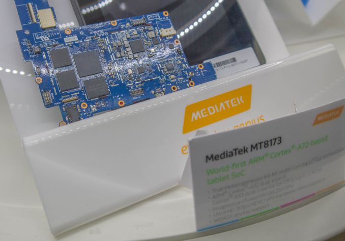
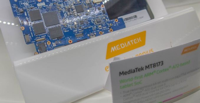
What was far the biggest surprise for us was the showing off of MT8173 hardware, a mid-range tablet SoC employing ARM’s new Cortex A72. It’s only been a few weeks since ARM officially announced the ARM Cortex A72, and while we still don’t know much about the micro-architectural nuances of the core, having MediaTek already displaying silicon is a severe departure from ARM’s usual announcement-to-release cadence. This puts the number A72 licensees with announced products already at two, with Qualcomm being the other one in the form of the Snapdragon 618 and 620.

The MT8173 employs two Cortex A72 CPUs at up to 2.4GHz and two Cortex A53 CPUs in a big.LITTLE configuration. On the GPU side we find a PowerVR GX6250 GPU, which if MediaTek’s clocking strategy continues should run north of 700MHz. The SoC is still powered by LPDDR3 as the preferred memory interface, undoubtedly a cost decision as we’re only starting to see LPDDR4 in flagship devices. On the multimedia side there’s MediaTek’s new display pipeline capable of 120Hz operation, 4K H.264/HEVC(10-bit)/VP9 video decoders and an ISP capable of 20MP sensors.

As part of the MWC announcements was also a (re)branding of MediaTek’s SoC lineup. Beginning with the MT6795 which is now denominated the Helio X10, MediaTek will in the future begin naming their new chips after the Helio (After the Greek word for sun, “helios”) brand. We’ll be seeing the P-line targeting the premium performance segment while the X-line targets the high-end and the best MediaTek has to offer.

MT3188: PMA, WPC and A4WP Wireless Charging Solution In 1

As part of the booth demos, MediaTek showed off the MT3188 wireless charging IC solution which supports all three currently available standards, PMA, WPC and the newly emerged A4WP standard. While we’ve had the IC announced early last year, it is still impressive to see the real thing in hardware.

WPC (Wireless Power Consortium) is by far the currently most widely available standard in the form of Qi, which has seen large adoption in the mobile space. PMA (Power Matters Alliance) remains as the competitor standard but which hasn’t seen as wide of an adoption rate with its Powermat/Duracell chargers. Both WPC and PMA rely on inductive charging which limit the spatial freedom between the transmitter and receiver coils to a few mm. 

A4WP on the other hand is the new standard which is based on resonance charging, giving devices the freedom in x, y and z directions around the emitter coil. The charging area can be much larger than in the inductive charging technologies and also allows for one charger to simultaneously charge multiple devices. The advantage of inductive charging over resonance charging remains in the efficiency and EMI aspects.

The demonstration of the A4WP standard was impressive as it allows for an enormous amount of flexibility in terms of integrating charging pads into furniture. Among multi-device charging bases, we also saw charging through relatively thick wooden tables where the charger was hidden underneath, instead of having to integrate them into the table of having a mat on lying on top.

The MT3188 joins other unified charging solutions such as Broadcomm’s BCM59350 which we also saw demonsrated at MWC this year.

MiraVision Display Pipeline Processing

Another interesting demo was the showing off of MiraVision integrated in MediaTek’s SoCs. Basically MiraVision is a fixed-function post-processor which sits on the display pipeline which has full control of the image data being sent to the display. The use-cases which MediaTek demonstrated were colour gamut manipulation on one side, something which is already for example done in products such as the Meizu MX4 with the MT6595. What was impressive to me was the dynamic analysis of image content in dark environments and subsequent adjusting of back-light and pixel data to allow for better visibility. Think of it as a dynamic gamma-curve adjustment.

There were a few demos, including a third-person shooter one where the effect was considerable to the viewing experience. We’ve seen Samsung employ similar technology in their Exynos and television SoCs called mDNIe (Mobile digital natural image enhancement) which used among other things to change between display profiles on Galaxy devices. MediaTek’s solution seems to one-up that as it allows for more dynamic settings as opposed to simply just having fixed programmed profiles.

MediaTek also demonstrated a frame-interpolation function for video playback through MiraVision. The result is similar to what SVP achieves in the PC space via software, but here it’s again implemented through fixed-function hardware to achieve high performance at very low power. Video content that is sourced at 24fps is interpolated to 60fps on the screen. The result is remarkable on a small screen as it suffers less from the “fake motion” that one associates with such techniques (Or MediaTek’s implementation is just really good?). 

The demo unit was again a Meizu MX4, so it means the hardware and products are already out there but just merely need to be officially adopted by the vendors in software.

MediaTek’s Modem Progression

Modems are an important part of MediaTek’s strategy and we’ve had more or less a status-update on how things are progressing. The LTE products from MediaTek are still far and few in-between that seems to be changing in the future as we’re seeing quick progression from the current Cat. 4 modem IP to Cat. 6 solutions in 2015 and Cat. 10 in 2016. 

An interesting addition is the adoption and field testing of C2K, or better known as CDMA2000. Other vendors such as Intel and Samsung chose not to adopt the technology as in the future we’ll see it being phased out in favour of LTE-only networks. For MediaTek to adopt it even though long-term it makes no sense, puts them in a unique position against Qualcomm in markets such as the US and China.

Broadcom at MWC 2015: BCM4359 and BCM43455 Wifi Combo Chips Announced

Broadcom at MWC 2015: BCM4359 and BCM43455 Wifi Combo Chips Announced

Today Broadcom took the lead by announcing two new Wifi combo chip solutions meant for the smartphone and tablet market. The BCM4359 is a high-end 2×2 MIMO solution for high-performance smartphones, while the BCM43455 is an updated 1×1 MIMO 802.11ac for mass market phones.

Taking a closer look at the BCM4359, we see several innovative new features, the most characterizing one being the inclusion for the first time of Real Simultaneous Dual Band (RSDB). RSDB enables the chip to connect to both 2.4GHz and 5GHz bands simultaneously. This is achieved by doubling up on the baseband processors on the combo chip. Broadcom uses ARM Cortex R4 as the processing units of the IC, and the 4359 uses two of them. What this enables is a sort of “full duplex” on the two frequency bands instead of having the baseband having to switch between each in an interleaving manner. The PHY bandwidth has been upped to 867 Mbps in the two-stream MIMO mode.

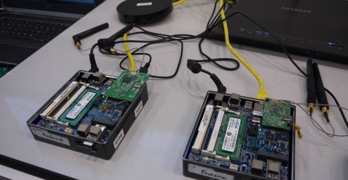
In the demo that Broadcom showed us, we had two test devices and a TV as the showcase setup. One device running the BCM4356 was streaming a video to the secondary device which employed the BCM4359 via the 2.4GHz band, who in turn would then stream via Wifi Display on 5GHz to the TV. As a comparison demo, we had the same setup next to it, but with both streaming devices equiped with only a BCM4356 solution. While the BCM4359 setup managed to achieve enough bandwidth to receive and forward the stream to the TV in full 1080p, the other side with the BCM4356 would only be fluid if the quality was reduced to 480p.

Another advantage of RSDB is that it enables the chip to scan for networks on both bands simultaneously, accelerating the time needed to show available Wifi networks, effectively giving a 2x speed improvement.

The BCM43455 is also a new member of the Broadcom family and serves as a solution for the mass market, meaning a cheaper price-point. It is a 1×1 HT80 802.11ac 2.4 and 5GHz solution, enabling up to a 433Mbps PHY rate at 80MHz channel bandwidth. The chip is able to reduce the BoM by 50%, although Broadcom didn’t specify to what this was compared with.

One key aspect of these new Wifi generation chips is that SDIO has been retired (but still available as a seconary option) as the connection interface to the SoC and instead replaced by PCIe. The BCM4358 was the first such chip to take advantage of this switch, which was employed on for example the Galaxy Note 4. The PCIe interface not only provides higher bandwidths which are beyond what SDIO is capable of, but also enables crucial power advantages such as low power states on the bus and bonuses such as Direct Memory Access (DMA) for the Wifi chipset.

Both the BCM4359 and BCM43455 are sampling now and will be available in devices later in the year.

Broadcom at MWC 2015: BCM4359 and BCM43455 Wifi Combo Chips Announced

Broadcom at MWC 2015: BCM4359 and BCM43455 Wifi Combo Chips Announced

Today Broadcom took the lead by announcing two new Wifi combo chip solutions meant for the smartphone and tablet market. The BCM4359 is a high-end 2×2 MIMO solution for high-performance smartphones, while the BCM43455 is an updated 1×1 MIMO 802.11ac for mass market phones.

Taking a closer look at the BCM4359, we see several innovative new features, the most characterizing one being the inclusion for the first time of Real Simultaneous Dual Band (RSDB). RSDB enables the chip to connect to both 2.4GHz and 5GHz bands simultaneously. This is achieved by doubling up on the baseband processors on the combo chip. Broadcom uses ARM Cortex R4 as the processing units of the IC, and the 4359 uses two of them. What this enables is a sort of “full duplex” on the two frequency bands instead of having the baseband having to switch between each in an interleaving manner. The PHY bandwidth has been upped to 867 Mbps in the two-stream MIMO mode.

In the demo that Broadcom showed us, we had two test devices and a TV as the showcase setup. One device running the BCM4356 was streaming a video to the secondary device which employed the BCM4359 via the 2.4GHz band, who in turn would then stream via Wifi Display on 5GHz to the TV. As a comparison demo, we had the same setup next to it, but with both streaming devices equiped with only a BCM4356 solution. While the BCM4359 setup managed to achieve enough bandwidth to receive and forward the stream to the TV in full 1080p, the other side with the BCM4356 would only be fluid if the quality was reduced to 480p.

Another advantage of RSDB is that it enables the chip to scan for networks on both bands simultaneously, accelerating the time needed to show available Wifi networks, effectively giving a 2x speed improvement.

The BCM43455 is also a new member of the Broadcom family and serves as a solution for the mass market, meaning a cheaper price-point. It is a 1×1 HT80 802.11ac 2.4 and 5GHz solution, enabling up to a 433Mbps PHY rate at 80MHz channel bandwidth. The chip is able to reduce the BoM by 50%, although Broadcom didn’t specify to what this was compared with.

One key aspect of these new Wifi generation chips is that SDIO has been retired (but still available as a seconary option) as the connection interface to the SoC and instead replaced by PCIe. The BCM4358 was the first such chip to take advantage of this switch, which was employed on for example the Galaxy Note 4. The PCIe interface not only provides higher bandwidths which are beyond what SDIO is capable of, but also enables crucial power advantages such as low power states on the bus and bonuses such as Direct Memory Access (DMA) for the Wifi chipset.

Both the BCM4359 and BCM43455 are sampling now and will be available in devices later in the year.

Qualcomm Announces New SoC Lineup, Modem Branding

Qualcomm Announces New SoC Lineup, Modem Branding

Qualcomm today announced 4 new additions to its Snapdragon 400 and 600 lineup of SoCs, along with a reshuffle and rebranding of their modem lineup. Let’s begin with the new SoC offerings:

The Snapdragon 415 and 425 are additions to the low-end of Qualcomm’s SoC offerings. The Snapdragon 415 is described a “quick transition piece” to the Snapdragon 410 which we suspect means it will be a pin-compatible SoC upgrade. It doubles up on the core-count from 4 A53 processors up to 8. The cores are still clocked in at the same 1.4GHz frequency. On the GPU side we see an upgrade from the Adreno 306 to a newer Adreno 405 and memory speeds have been slightly bumped from 533MHz to 667MHz LPDDR3, dropping LPDDR2 capability from the SKU.

Qualcomm Snapdragon 400 Lineup
SoC Snapdragon 410 Snapdragon 415 Snapdragon 425
CPU 4x Cortex [email protected] 4x Cortex A53@?GHz

4x Cortex [email protected]

4x Cortex A53@?GHz

4x Cortex [email protected]

Memory
Controller
1x 32-bit @ 533MHz
LPDDR2/3

4.2GB/s b/w

1x 32-bit @ 667MHz
LPDDR3

5.3GB/s b/w

1x 32-bit @ 933MHz
LPDDR3

7.5GB/s b/w

GPU Adreno 306 Adreno 405 Adreno 405
Encode/
Decode
1080p H.264 1080p H.264

1080p30 HEVC decode

1080p H.264

1080p30 HEVC decode

Camera/ISP 13.5MP 13MP Dual ISP
21MP
Integrated
Modem
Cat. 4 150Mbps “X5 LTE” Cat. 4
150Mbps DL
50Mbps UL
“X8 LTE” Cat. 7 
300Mbps DL 100Mbps UL

2x20MHz C.A.
(DL & UL)

The Snapdragon 425 is also a octa-core A53 unit with the same GPU implementation, but clocked at a slightly higher 1.7GHz on the one of the A53 clusters. It’s on the integrated modem side where things change, as the S425 employs a new integrated “X8 LTE” Category 7 LTE modem versus the Category 4 one found in the S415. The new unit also brings down the dual-ISP feature from the higher-end SoCs to the entry-level, enabling dual cameras up to 21MP. This should be an interesting SoC in the entry range as the specifications in terms of performance seem to match the Snapdragon 615 of the mid-range series.

While the entry range gets some large performance and connectivity boosts, today’s biggest news comes in form of the Snapdragon 618 and 620. These are the first announced Cortex A72 SoCs, ARM’s new high-end CPU architecture which was publicly announced just two weeks ago.

Qualcomm Snapdragon 600 Lineup
SoC Snapdragon 610 Snapdragon 615 Snapdragon 618 Snapdragon 620
CPU 4x Cortex [email protected] 4x Cortex A53 @1.0GHz

4x Cortex A53 @1.7GHz

4x Cortex A53 @1.2GHz

2x Cortex A72 @1.8GHz

4x Cortex A53 @1.2GHz

4x Cortex A72 @1.8GHz

Memory
Controller
1x 32-bit @ 800MHz
LPDDR3

6.4GB/s b/w

1x 32-bit @ 800MHz
LPDDR3

6.4GB/s b/w

2x 32-bit @ 933MHz
LPDDR3

14.9GB/s b/w

2x 32-bit @ 933MHz
LPDDR3

14.9GB/s b/w

GPU Adreno 405 Adreno 405 “Next-gen” Adreno “Next-gen” Adreno
Encode/
Decode
1080p H.264

1080p30 HEVC decode

1080p H.264

1080p30 HEVC decode

2160p30, 1080p120
H.264 & HEVC
2160p30, 1080p120
H.264 & HEVC
Camera/ISP 21MP 13MP Dual ISP
21MP
Dual ISP
21MP
Integrated
Modem
Cat. 4
150Mbps DL
50Mbps UL
“X5 LTE” Cat. 4
150Mbps DL
50Mbps UL
“X8 LTE” Cat. 7
300Mbps DL 100Mbps UL

2x20MHz C.A. 
(DL & UL)

“X8 LTE” Cat. 7 
300Mbps DL 100Mbps UL

2x20MHz C.A. 
(DL & UL)

The Snapdragon 618 and 620 bring dual-channel memory back into the mid-range, employing LPDDR3 targeted at 933MHz, making them on par with today’s Snapdragon 800 and 801 SoCs. The new offerings now employ full HEVC (H.265) hardware encoding and decoding, a feature first seen in the Snapdragon 810. Similarly to the 425, the usually high-end dual ISP functionality is brought down into the new SKUs and offer up to 21MP camera sensor functionality.

What Qualcomm doesn’t specify though, is the GPU. We’re being promised a new “next-generation” Adreno GPU, so we might be talking about a new 500-series, but we don’t know for sure until Qualcomm actually announces the new architecture.

The Snapdragon 618 and 620 employ Qualcomm’s new “X8” integrated modem solutions, capable of Category 7 LTE with up to 300Mbps downstream or 100Mbps upstream via 2x20MHz carrier aggregation on either upload or download channels.

Getting back to the CPU configuration: The Cortex A72 replaces the use of a higher-clocked A53 cluster as the “big” part of these new big.LITTLE SoCs. The A72 was announced as ARM’s new flagship high-end core, so it’s very interesting to see Qualcomm employ it in a mid-range SoC at only 1.8GHz. It would look like these new units are still manufactured under 28nm given the clock speeds. We still don’t know much about the A72 core, but ARM’s Peter Greenhalgh clarified that we should be seeing a 10-50% IPC gain over the A57 while improving power on the same process node and libraries. To see Qualcomm use the A72 in a mid-range SoC begs the question of exactly how big these new cores are, as pricing is be an important competitive factor below the high-end.

Qualcomm expects the Snapdragon 415, 425, 618 and 620 to ship in consumer devices in the latter half of 2015. This is an interesting timeline as the 618 and 620 pose direct competition to the Snapdragon 808 which we still haven’t seen announced in any consumer device. On the high-end, Qualcomm is still keeping very quiet as we still don’t know what the successor to the Snapdragon 810 will look like or what the state of Qualcomm’s new ARMv8 core is in. 

Modem re-branding

Finally as part of today’s announcement, is a re-branding of Qualcomm’s modem line-up. The “Gobi” name is abandoned in favour of a “X# LTE” denomination. It’s to be noted that the model numbers don’t correspond to actual LTE category capability, as for example the X10 and X12 modems are capable of respectively Category 9 and 10 LTE. The aforementioned parts are re-brandings of the modem variants which we find in the standalone Gobi 9×45 and 9×40 and Snapdragon 808 and 810 SoCs.

Today Qualcomm raised the bar for low- and mid-range SoCs and we’re looking forward to what kind devices Qualcomm’s OEM partners will come up with towards the end of the year.

Source (Qualcomm)

Qualcomm Announces New SoC Lineup, Modem Branding

Qualcomm Announces New SoC Lineup, Modem Branding

Qualcomm today announced 4 new additions to its Snapdragon 400 and 600 lineup of SoCs, along with a reshuffle and rebranding of their modem lineup. Let’s begin with the new SoC offerings:

The Snapdragon 415 and 425 are additions to the low-end of Qualcomm’s SoC offerings. The Snapdragon 415 is described a “quick transition piece” to the Snapdragon 410 which we suspect means it will be a pin-compatible SoC upgrade. It doubles up on the core-count from 4 A53 processors up to 8. The cores are still clocked in at the same 1.4GHz frequency. On the GPU side we see an upgrade from the Adreno 306 to a newer Adreno 405 and memory speeds have been slightly bumped from 533MHz to 667MHz LPDDR3, dropping LPDDR2 capability from the SKU.

Qualcomm Snapdragon 400 Lineup
SoC Snapdragon 410 Snapdragon 415 Snapdragon 425
CPU 4x Cortex [email protected] 4x Cortex A53@?GHz

4x Cortex [email protected]

4x Cortex A53@?GHz

4x Cortex [email protected]

Memory
Controller
1x 32-bit @ 533MHz
LPDDR2/3

4.2GB/s b/w

1x 32-bit @ 667MHz
LPDDR3

5.3GB/s b/w

1x 32-bit @ 933MHz
LPDDR3

7.5GB/s b/w

GPU Adreno 306 Adreno 405 Adreno 405
Encode/
Decode
1080p H.264 1080p H.264

1080p30 HEVC decode

1080p H.264

1080p30 HEVC decode

Camera/ISP 13.5MP 13MP Dual ISP
21MP
Integrated
Modem
Cat. 4 150Mbps “X5 LTE” Cat. 4
150Mbps DL
50Mbps UL
“X8 LTE” Cat. 7 
300Mbps DL 100Mbps UL

2x20MHz C.A.
(DL & UL)

The Snapdragon 425 is also a octa-core A53 unit with the same GPU implementation, but clocked at a slightly higher 1.7GHz on the one of the A53 clusters. It’s on the integrated modem side where things change, as the S425 employs a new integrated “X8 LTE” Category 7 LTE modem versus the Category 4 one found in the S415. The new unit also brings down the dual-ISP feature from the higher-end SoCs to the entry-level, enabling dual cameras up to 21MP. This should be an interesting SoC in the entry range as the specifications in terms of performance seem to match the Snapdragon 615 of the mid-range series.

While the entry range gets some large performance and connectivity boosts, today’s biggest news comes in form of the Snapdragon 618 and 620. These are the first announced Cortex A72 SoCs, ARM’s new high-end CPU architecture which was publicly announced just two weeks ago.

Qualcomm Snapdragon 600 Lineup
SoC Snapdragon 610 Snapdragon 615 Snapdragon 618 Snapdragon 620
CPU 4x Cortex [email protected] 4x Cortex A53 @1.0GHz

4x Cortex A53 @1.7GHz

4x Cortex A53 @1.2GHz

2x Cortex A72 @1.8GHz

4x Cortex A53 @1.2GHz

4x Cortex A72 @1.8GHz

Memory
Controller
1x 32-bit @ 800MHz
LPDDR3

6.4GB/s b/w

1x 32-bit @ 800MHz
LPDDR3

6.4GB/s b/w

2x 32-bit @ 933MHz
LPDDR3

14.9GB/s b/w

2x 32-bit @ 933MHz
LPDDR3

14.9GB/s b/w

GPU Adreno 405 Adreno 405 “Next-gen” Adreno “Next-gen” Adreno
Encode/
Decode
1080p H.264

1080p30 HEVC decode

1080p H.264

1080p30 HEVC decode

2160p30, 1080p120
H.264 & HEVC
2160p30, 1080p120
H.264 & HEVC
Camera/ISP 21MP 13MP Dual ISP
21MP
Dual ISP
21MP
Integrated
Modem
Cat. 4
150Mbps DL
50Mbps UL
“X5 LTE” Cat. 4
150Mbps DL
50Mbps UL
“X8 LTE” Cat. 7
300Mbps DL 100Mbps UL

2x20MHz C.A. 
(DL & UL)

“X8 LTE” Cat. 7 
300Mbps DL 100Mbps UL

2x20MHz C.A. 
(DL & UL)

The Snapdragon 618 and 620 bring dual-channel memory back into the mid-range, employing LPDDR3 targeted at 933MHz, making them on par with today’s Snapdragon 800 and 801 SoCs. The new offerings now employ full HEVC (H.265) hardware encoding and decoding, a feature first seen in the Snapdragon 810. Similarly to the 425, the usually high-end dual ISP functionality is brought down into the new SKUs and offer up to 21MP camera sensor functionality.

What Qualcomm doesn’t specify though, is the GPU. We’re being promised a new “next-generation” Adreno GPU, so we might be talking about a new 500-series, but we don’t know for sure until Qualcomm actually announces the new architecture.

The Snapdragon 618 and 620 employ Qualcomm’s new “X8” integrated modem solutions, capable of Category 7 LTE with up to 300Mbps downstream or 100Mbps upstream via 2x20MHz carrier aggregation on either upload or download channels.

Getting back to the CPU configuration: The Cortex A72 replaces the use of a higher-clocked A53 cluster as the “big” part of these new big.LITTLE SoCs. The A72 was announced as ARM’s new flagship high-end core, so it’s very interesting to see Qualcomm employ it in a mid-range SoC at only 1.8GHz. It would look like these new units are still manufactured under 28nm given the clock speeds. We still don’t know much about the A72 core, but ARM’s Peter Greenhalgh clarified that we should be seeing a 10-50% IPC gain over the A57 while improving power on the same process node and libraries. To see Qualcomm use the A72 in a mid-range SoC begs the question of exactly how big these new cores are, as pricing is be an important competitive factor below the high-end.

Qualcomm expects the Snapdragon 415, 425, 618 and 620 to ship in consumer devices in the latter half of 2015. This is an interesting timeline as the 618 and 620 pose direct competition to the Snapdragon 808 which we still haven’t seen announced in any consumer device. On the high-end, Qualcomm is still keeping very quiet as we still don’t know what the successor to the Snapdragon 810 will look like or what the state of Qualcomm’s new ARMv8 core is in. 

Modem re-branding

Finally as part of today’s announcement, is a re-branding of Qualcomm’s modem line-up. The “Gobi” name is abandoned in favour of a “X# LTE” denomination. It’s to be noted that the model numbers don’t correspond to actual LTE category capability, as for example the X10 and X12 modems are capable of respectively Category 9 and 10 LTE. The aforementioned parts are re-brandings of the modem variants which we find in the standalone Gobi 9×45 and 9×40 and Snapdragon 808 and 810 SoCs.

Today Qualcomm raised the bar for low- and mid-range SoCs and we’re looking forward to what kind devices Qualcomm’s OEM partners will come up with towards the end of the year.

Source (Qualcomm)