Mobile


Qualcomm Snapdragon 820 Experience: HMP Kryo and Demos

Qualcomm Snapdragon 820 Experience: HMP Kryo and Demos

While the Snapdragon 820 has had a number of announcements about various aspects of the SoC, some details have been mostly left to the imagination. Today, Qualcomm held an event to release some details about Snapdragon 820, but also to show off what can be enabled by Snapdragon 820. Some of the main details released today include some estimates of power, and some additional disclosure on the Kryo CPU cores in Snapdragon 820.

In power, Qualcomm published a slide showing average power consumption using their own internal model for determining days of use. In their testing, it shows that Snapdragon 820 uses 30% less power for the same time of use. Of course, this needs to be taken with appropriate skepticism, but given the use of 14LPP it probably shouldn’t be a surprise that Snapdragon 820 improves significantly over past devices.

The other disclosures of note were primarily centered on the CPU and modem. On the modem side, Qualcomm is claiming 15% improvement in power efficiency which should eliminate any remaining gap between LTE and WiFi battery life.

On the CPU side, while the claims of either doubled performance or power efficiency have been discussed before, new details on the CPU include that the quad core CPU is best described as an HMP solution with two high-performance cores clocked at 2.2 GHz and two low-power cores clocked at 1.6 or 1.7GHz when looking at previous Qualcomm SoCs with two clusters that share an architecture. Qualcomm also disclosed that the CPU architectures of both clusters are identical, but with differences in cache configuration. However, the differences in cache configuration weren’t disclosed. I wasn’t able to get an answer regarding whether this is an ARM big.LITTLE design that uses CCI-400 or CCI-500, but given that there’s an L3 cache shared between clusters it’s more likely that this is a completely custom HMP architecture.

In addition to these disclosures, we saw a number of demos. Probably the single most interesting demo shown was Sense ID, in which it was shown that fingerprint sensing worked properly through a sheet of glass and aluminum. To my recollection both the glass and aluminum were 0.4mm thick, so the system seems to be relatively robust. For those unfamiliar with Sense ID, rather than relying of high-resolution capacitive touch sensing the system uses ultrasonic sound waves to map the fingerprint, which allows it to penetrate materials like glass and metal and improves sensitivity despite contaminants like water and dirt.

One area of note was that Qualcomm is now offering their own speaker amp/protection IC that would compete with ICs like the NXP TFA9895 that are quite common in devices today. The WSA8815 chip would also be able to deliver stereo sound effects in devices with stereo front-facing speakers. It seems that the primary advantage of this solution is cost when bundled with the SoC, but it remains to be seen whether OEM adoption would be widespread.

One of the other demos was improved low light video and photos by using the Hexagon 680 DSP and Spectra 14-bit dual ISP. The main area of interest in this demo was improved visibility of underexposed areas by boosting shadow visibility, while also eliminating the resulting noise through temporal noise reduction.

On the RF side, in addition to showing that the Snapdragon 820 modem is capable of UE Category 12/13 LTE speeds Qualcomm also demonstrated that the Snapdragon 820 is capable of dynamically detecting WiFi signal quality based upon throughput and other metrics that affect VOIP quality and seamlessly handing off calls from WiFi to LTE and back. We also saw a demo for Qualcomm’s closed-loop antenna tuning system which allows for reduced impedance mismatch relative to previous open-loop antenna tuners which loaded various antenna profiles based upon things like touch sensing of certain critical areas.

Imagination Announces New P6600, M6200, M6250 Warrior CPUs

Imagination Announces New P6600, M6200, M6250 Warrior CPUs

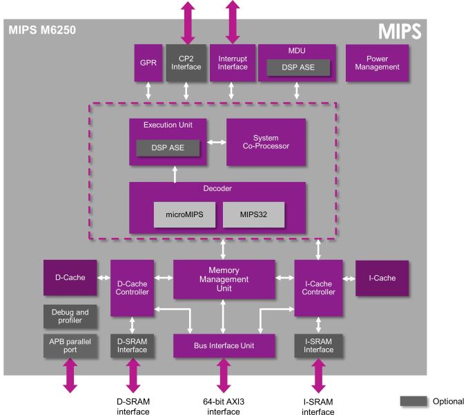
Today Imagination launches three new MIPS processor IPs: One in the performance category of Warrior CPUs, the P6600 and two embedded M-class core, the M6200 and M6250.

Warrior P6600

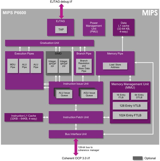
Starting off with the P6600, this is Imagination’s new MIPS flagship core succeeding the P5600. The P5600 was a 3-wide out-of-order design with a pipeline depth of up to 16 stages. The P6600 keeps most of the predecessor’s characteristics such as the main architectural features or full hardware virtualization and security through OmniShield, but adds compatibility for MIPS64 64-bit processing on top. Imagination first introduced a mobile oritented 64-bit MIPS CPU back with the I6400 a little more than a year ago but we’ve yet to see vendors announce products with it. 

We’re still lacking any details on the architectural improvements of the P6600 over the P5600 so it seems that for now we’re left with guessing what kind of performance the new core will bring. The P5600 was directly competing with ARM’s Cortex A15 in terms of IPC, but ARM has since then not only announced but also seen silicon with two successor IPs to the A15 (A57 and A72), so the P6600 will have some tough competition ahead of itself once it arrives in products.

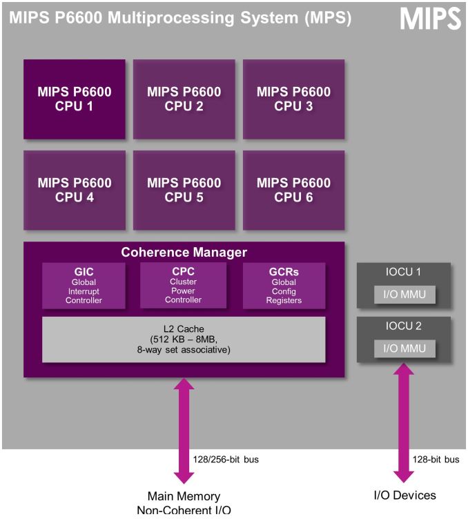
The P6600, much like the P5600 can be implemented from single-core to six-core cluster configurations. What is interesting that as opposed to ARM CPU IP, the MIPS cores allow for asynchronous clock planes between the individual cores if the vendors wishes to implement the SoC’s power management in this way (It can also be set up to work in a synchronous way).

“MIPS P6600 is the next evolution of the high-end MIPS P-class family and builds on the 32-bit P5600 CPU. P6600 is a balanced CPU for mainstream/high-performance computing, enabling powerful multicore 64-bit SoCs with optimal area efficiency for applications in segments including mobile, home entertainment, networking, automotive, HPC or servers, and more. Customers have already licensed the P6600 for applications including high-performance computing and advanced image and vision systems.”

Warrior M6200 & M6250

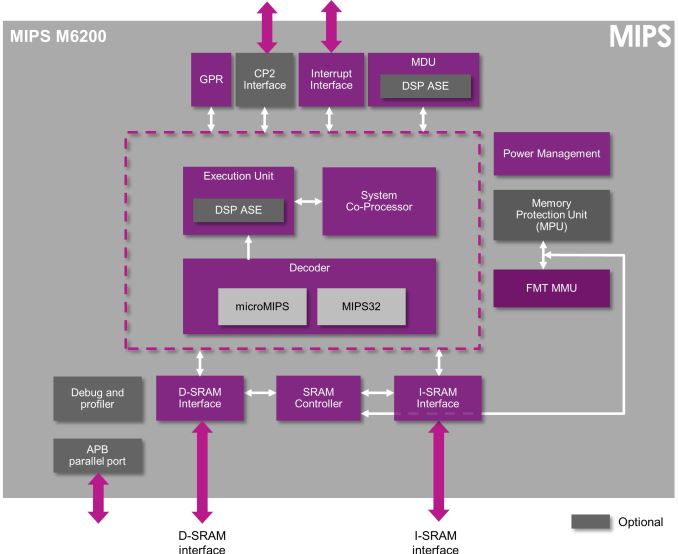
Also as part of today’s announcement we see two new embedded CPU cores, the M6200 and M6250. Both cores are successors to the microAptiv-UP and UC but able to run at up to 30% higher frequency. The new processors also see an ISA upgrade to MIPS32 Release 6 instead of Release 5.

The M6200 is targeted at real-time embedded operating systems with minimal funtionality for cost- and power-savings. It has no MMU and as such can only be described as a microcontroller part.

The M6250 is the bigger brother of the M6200 and the biggest difference is the inclusion of a memory management unit (MMU) that makes this a full fledged processor core that can run operating systems like Linux.

“M6200 and M6250 are configurable and fully synthesizable solutions for devices requiring a high level of performance efficiency and small silicon area including wireless or wired modems, GPU supervisors, flash and SSD controllers, industrial and motor control, advanced audio and more.”

Imagination Announces New P6600, M6200, M6250 Warrior CPUs

Imagination Announces New P6600, M6200, M6250 Warrior CPUs

Today Imagination launches three new MIPS processor IPs: One in the performance category of Warrior CPUs, the P6600 and two embedded M-class core, the M6200 and M6250.

Warrior P6600

Starting off with the P6600, this is Imagination’s new MIPS flagship core succeeding the P5600. The P5600 was a 3-wide out-of-order design with a pipeline depth of up to 16 stages. The P6600 keeps most of the predecessor’s characteristics such as the main architectural features or full hardware virtualization and security through OmniShield, but adds compatibility for MIPS64 64-bit processing on top. Imagination first introduced a mobile oritented 64-bit MIPS CPU back with the I6400 a little more than a year ago but we’ve yet to see vendors announce products with it. 

We’re still lacking any details on the architectural improvements of the P6600 over the P5600 so it seems that for now we’re left with guessing what kind of performance the new core will bring. The P5600 was directly competing with ARM’s Cortex A15 in terms of IPC, but ARM has since then not only announced but also seen silicon with two successor IPs to the A15 (A57 and A72), so the P6600 will have some tough competition ahead of itself once it arrives in products.

The P6600, much like the P5600 can be implemented from single-core to six-core cluster configurations. What is interesting that as opposed to ARM CPU IP, the MIPS cores allow for asynchronous clock planes between the individual cores if the vendors wishes to implement the SoC’s power management in this way (It can also be set up to work in a synchronous way).

“MIPS P6600 is the next evolution of the high-end MIPS P-class family and builds on the 32-bit P5600 CPU. P6600 is a balanced CPU for mainstream/high-performance computing, enabling powerful multicore 64-bit SoCs with optimal area efficiency for applications in segments including mobile, home entertainment, networking, automotive, HPC or servers, and more. Customers have already licensed the P6600 for applications including high-performance computing and advanced image and vision systems.”

Warrior M6200 & M6250

Also as part of today’s announcement we see two new embedded CPU cores, the M6200 and M6250. Both cores are successors to the microAptiv-UP and UC but able to run at up to 30% higher frequency. The new processors also see an ISA upgrade to MIPS32 Release 6 instead of Release 5.

The M6200 is targeted at real-time embedded operating systems with minimal funtionality for cost- and power-savings. It has no MMU and as such can only be described as a microcontroller part.

The M6250 is the bigger brother of the M6200 and the biggest difference is the inclusion of a memory management unit (MMU) that makes this a full fledged processor core that can run operating systems like Linux.

“M6200 and M6250 are configurable and fully synthesizable solutions for devices requiring a high level of performance efficiency and small silicon area including wireless or wired modems, GPU supervisors, flash and SSD controllers, industrial and motor control, advanced audio and more.”

ARM Announces New CCI-550 and DMC-500 System IPs

ARM Announces New CCI-550 and DMC-500 System IPs

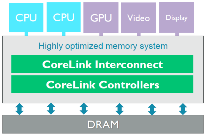
Today ARM announces two new additions to its CoreLink system IP design portfolio, the CCI-550 interconnect and DMC-500 memory controller. Starting off with the CCI announcement, we find the third iteration of the Cache Coherent Interconnect. The CCI is the cornerstone of ARM’s big.LITTLE strategy as it provides the required cache-coherent system interconnect between CPU clusters and other SoC blocks such as the main memory controllers and thus enabling heterogeneous multiprocessing between all the IP blocks.

The CCI-550 is an improvement to the CCI-500 which ARM announced back in February among other IPs such as the new Cortex A72 core design. Both the CCI-500 and the new CCI-550 are generational successors to the CCI-400 that is found in all currently released big.LITTLE SoCs such as Samsung’s Exynos, MediaTek’s Helio or Qualcomm’s Snapdragon designs. Back in February I was pretty excited to see ARM improve this part of their IP portfolio as it seemed that there was a lot of optimization that could be done in terms of performance and power.

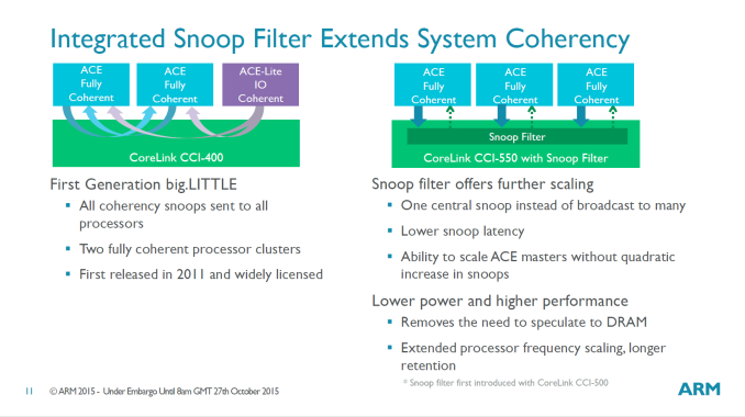
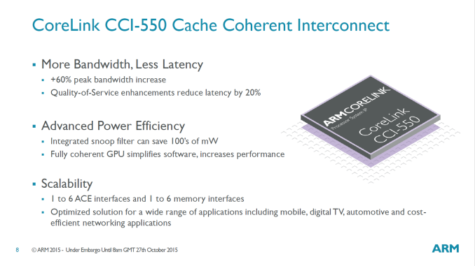
As a reminder, the primary characteristics of the new CCI-5X0 designs is the addition of a snoop filter within the interconnect that is able to maintain a directory of all cache contents among its coherent agents. On previous IP such as the CCI-400, all coherency messages needed to be broadcasted among all agents, causing them to have to wake up and respond. This not only impacted performance due to the increased latency but also had a power impact caused by the processing overhead. For the new CCI family, ARM explains that in heavy use-cases the new snoop filter can save up to “100’s” of milliwatts of power which is a quite significant figure.

Due the broadcast nature of how the CCI-400 was operated, it meant that adding another coherent agent would have incurred a quadratical increase in the amount of messages such as snoop lookups. The CCI-500 on the other hand is able to take advantage of the new filter to increase the number of ACE (AXI Coherency Extension) master ports from 2 to 4 without increased overhead. This for example enabled the implementation of up to 4 CPU clusters if a vendor wished to do so. The new CCI-550 again improves this configuration option by raising the maximum number of ACE master ports to up to 6.

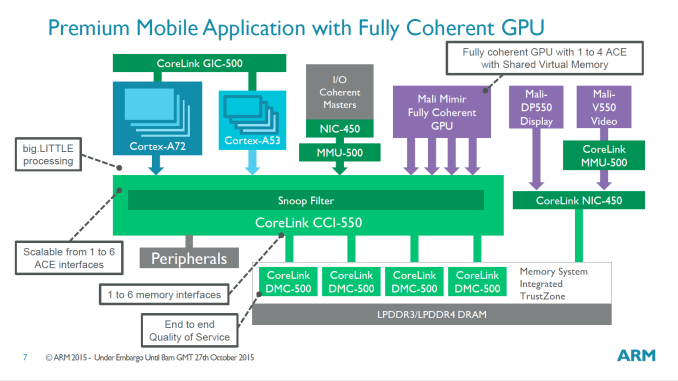
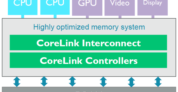
In the example SoC layout diagram that ARM provides, we see the CCI-550 configured with two CPU clusters such as the Cortex A53 and a Cortex A72. The remaining four ACE master ports could be then dedicated to a fully coherent GPU.

ARM explains that its still to-be-announced next-generation Mali IP codenamed “Mimir” will be fully cache-coherent and would be a perfect fit to take advantage of such a configuration (Current generation Midgard-based GPUs such as the T6-/7-/800 series are only I/O coherent). Fully coherent GPUs will be able to take advantage of shared virtual memory and new simplified programmers models provided by APIs such as OpenCL 2.0 and HSA.

While the amount of ACE master ports increases from 4 to 6, the amount of possible memory interfaces has also gone up from a maximum of 4 to up to 6. This allows an increase of up to 60% in the total peak interconnect bandwidth (total aggregate bandwidth). This improvement not only comes from the two additional memory interfaces, but also an additional increase which can be credited to micro-architectural improvements on the interconnect itself. For example, we’re told the CCI-550 is able to reduce CPU-to-memory latency by 20% when compared to the CCI-500.

ARM explains that its CCI IP is highly customizable and thus each vendor can configure it to their needs. The IP will be able to scale in terms of physical implementation based on the number of desired interfaces and ports.

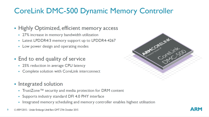
As an IP vendor, ARM is aiming to provide highly optimized integrated solutions, and memory controllers are consequently part of such designs. ARM previously offered the DMC-520 with DDR4 support but this memory controller was aimed at more complex enterprise designs employing AMBA 5 system IP such as ARM’s CCN (Cache Coherent Network). The DMC-500 announced today on the other hand is ARM’s first mobile-targeted memory controller with support for the new LPDDR4 memory standard. Aimed for AMBA 4 system IPs such as the CCI family, this is the memory controller IP we’ll most likely see adopted by vendors in consumer devices such as smartphones.

The DMC-500 promises support for LPDDR4 up to 2133MHz while still maintaining LPDDR3 compatibility. This is an important differentiation factor as in doing so ARM is able to offer maximum flexibility in terms of choice of implementation for vendors. Performance wise, ARM promises up to 27% increase in memory bandwidth utilization in a low power design.

All in all today’s announcements provide some solid improvements in ARM’s IP portfolio. On the memory controller side I’m not certain what the rate of adoption ARM’s DMC’s is; as far as I know the main “heavyweight” SoC vendors currently chose to employ their own memory controller IP. Those who don’t have their own IP and instead use ARM’s designs are often hard to single out as many times the choice of memory controller is completely invisible to the system.

On the interconnect side I predict that we’ll be seeing a lot more discussions and developments from third-party vendors. Even among today’s higher-profile big.LITTLE SoCs I’m only aware of LG’s Odin to use ARM’s CCI as a “center-piece” in their SoC fabric while other vendors such as Samsung chose to implement it alongside their own interconnect fabric. Vendors who have the resources and design talent may also chose to implement cache coherency into their own interconnect IP. They would thus be able deploy big.LITTLE systems or other similar fully coherent SoCs without ARM’s CCI IP. For example, MediaTek is among the first to do exactly this in the Helio X20 with help of the in-house designed MCSI. Next year we should be seeing new big.LITTLE SoCs equipped with both ARM’s IP such as the CCI-500 or 550 alongside third-party IP, creating a new differentiation point for SoC vendors that will undoubtedly make competitive landscape much more interesting.

ARM Announces New CCI-550 and DMC-500 System IPs

ARM Announces New CCI-550 and DMC-500 System IPs

Today ARM announces two new additions to its CoreLink system IP design portfolio, the CCI-550 interconnect and DMC-500 memory controller. Starting off with the CCI announcement, we find the third iteration of the Cache Coherent Interconnect. The CCI is the cornerstone of ARM’s big.LITTLE strategy as it provides the required cache-coherent system interconnect between CPU clusters and other SoC blocks such as the main memory controllers and thus enabling heterogeneous multiprocessing between all the IP blocks.

The CCI-550 is an improvement to the CCI-500 which ARM announced back in February among other IPs such as the new Cortex A72 core design. Both the CCI-500 and the new CCI-550 are generational successors to the CCI-400 that is found in all currently released big.LITTLE SoCs such as Samsung’s Exynos, MediaTek’s Helio or Qualcomm’s Snapdragon designs. Back in February I was pretty excited to see ARM improve this part of their IP portfolio as it seemed that there was a lot of optimization that could be done in terms of performance and power.

As a reminder, the primary characteristics of the new CCI-5X0 designs is the addition of a snoop filter within the interconnect that is able to maintain a directory of all cache contents among its coherent agents. On previous IP such as the CCI-400, all coherency messages needed to be broadcasted among all agents, causing them to have to wake up and respond. This not only impacted performance due to the increased latency but also had a power impact caused by the processing overhead. For the new CCI family, ARM explains that in heavy use-cases the new snoop filter can save up to “100’s” of milliwatts of power which is a quite significant figure.

Due the broadcast nature of how the CCI-400 was operated, it meant that adding another coherent agent would have incurred a quadratical increase in the amount of messages such as snoop lookups. The CCI-500 on the other hand is able to take advantage of the new filter to increase the number of ACE (AXI Coherency Extension) master ports from 2 to 4 without increased overhead. This for example enabled the implementation of up to 4 CPU clusters if a vendor wished to do so. The new CCI-550 again improves this configuration option by raising the maximum number of ACE master ports to up to 6.

In the example SoC layout diagram that ARM provides, we see the CCI-550 configured with two CPU clusters such as the Cortex A53 and a Cortex A72. The remaining four ACE master ports could be then dedicated to a fully coherent GPU.

ARM explains that its still to-be-announced next-generation Mali IP codenamed “Mimir” will be fully cache-coherent and would be a perfect fit to take advantage of such a configuration (Current generation Midgard-based GPUs such as the T6-/7-/800 series are only I/O coherent). Fully coherent GPUs will be able to take advantage of shared virtual memory and new simplified programmers models provided by APIs such as OpenCL 2.0 and HSA.

While the amount of ACE master ports increases from 4 to 6, the amount of possible memory interfaces has also gone up from a maximum of 4 to up to 6. This allows an increase of up to 60% in the total peak interconnect bandwidth (total aggregate bandwidth). This improvement not only comes from the two additional memory interfaces, but also an additional increase which can be credited to micro-architectural improvements on the interconnect itself. For example, we’re told the CCI-550 is able to reduce CPU-to-memory latency by 20% when compared to the CCI-500.

ARM explains that its CCI IP is highly customizable and thus each vendor can configure it to their needs. The IP will be able to scale in terms of physical implementation based on the number of desired interfaces and ports.

As an IP vendor, ARM is aiming to provide highly optimized integrated solutions, and memory controllers are consequently part of such designs. ARM previously offered the DMC-520 with DDR4 support but this memory controller was aimed at more complex enterprise designs employing AMBA 5 system IP such as ARM’s CCN (Cache Coherent Network). The DMC-500 announced today on the other hand is ARM’s first mobile-targeted memory controller with support for the new LPDDR4 memory standard. Aimed for AMBA 4 system IPs such as the CCI family, this is the memory controller IP we’ll most likely see adopted by vendors in consumer devices such as smartphones.

The DMC-500 promises support for LPDDR4 up to 2133MHz while still maintaining LPDDR3 compatibility. This is an important differentiation factor as in doing so ARM is able to offer maximum flexibility in terms of choice of implementation for vendors. Performance wise, ARM promises up to 27% increase in memory bandwidth utilization in a low power design.

All in all today’s announcements provide some solid improvements in ARM’s IP portfolio. On the memory controller side I’m not certain what the rate of adoption ARM’s DMC’s is; as far as I know the main “heavyweight” SoC vendors currently chose to employ their own memory controller IP. Those who don’t have their own IP and instead use ARM’s designs are often hard to single out as many times the choice of memory controller is completely invisible to the system.

On the interconnect side I predict that we’ll be seeing a lot more discussions and developments from third-party vendors. Even among today’s higher-profile big.LITTLE SoCs I’m only aware of LG’s Odin to use ARM’s CCI as a “center-piece” in their SoC fabric while other vendors such as Samsung chose to implement it alongside their own interconnect fabric. Vendors who have the resources and design talent may also chose to implement cache coherency into their own interconnect IP. They would thus be able deploy big.LITTLE systems or other similar fully coherent SoCs without ARM’s CCI IP. For example, MediaTek is among the first to do exactly this in the Helio X20 with help of the in-house designed MCSI. Next year we should be seeing new big.LITTLE SoCs equipped with both ARM’s IP such as the CCI-500 or 550 alongside third-party IP, creating a new differentiation point for SoC vendors that will undoubtedly make competitive landscape much more interesting.