Mobile


Qualcomm Announces Snapdragon 625, 425 & 435 Mid- and Low-End SoCs

Qualcomm Announces Snapdragon 625, 425 & 435 Mid- and Low-End SoCs

Today Qualcomm announced three new SoCs in the mid and low-end Snapdragon lineup. At the lowest end we find the Snapdragon 425 offering a very frugal CPU configuration consisting of 4x Cortex A53’s clocked in at 1.4GHz. The chipset is aimed at replacing the Snapdragon 410 and 412 and improves on them with an upgrade on the modem block as well as media decoder and encoder capabilities, now enabling 1080p HEVC decode and encode.

The Snapdragon 435 replaces the Snapdragon 430 which was only announced just a few months ago and also sees an improvement in the modem block used as we see it now going from UE Category 4 to UE Category 7. On the CPU side we see a 200MHz boost in the frequency of the faster of the two quad-core A53 clusters, now reaching 1.4GHz. In both the Snapdragon 425 and 435 we don’t see a change in the GPU but it’s possible clocks have changed; unfortunately details on the matter are still sparse. Both the Snapdragon 425 and 435 are manufactured on a “28nm LP” process but sadly it wasn’t specified which foundry is manufacturing them.

New 2016 Mid & Low-End Snadpragons
SoC Snapdragon 425
(MSM8917)
Snapdragon 435
(MSM8940)
Snapdragon 625
(MSM8953)
CPU 4x A53 @ 1.4GHz 4x A53 @ 1.4GHz

4x A53 @ ? GHz

4x A53 @ 2.0GHz

4x A53 @ ? GHz

Memory 1x 32-bit @ 667MHz
LPDDR3

5.3GB/s b/w

1x 32-bit @ 800MHz
LPDDR3

6.4GB/s b/w

1x 32-bit @ 933MHz
LPDDR3

7.45GB/s b/w

GPU Adreno 308 Adreno 505 Adreno 506
Encode/
Decode
1080p
H.264 & HEVC (Decode)
2160p
H.264 & HEVC (Decode)
Camera/ISP Dual ISP
16MP
Dual ISP
21MP
Dual ISP
24MP
Integrated
Modem
“X6 LTE” Cat. 4
150Mbps DL 75Mbps UL

2x20MHz C.A. 
(DL & UL)

“X8 LTE” Cat. 7
300Mbps DL 100Mbps UL

2x20MHz C.A. 
(DL & UL)

“X9 LTE” Cat. 7
300Mbps DL 150Mbps UL

2x20MHz C.A. 
(DL & UL)

Mfc. Process 28nm LP 14nm LPP

Most importantly comes the announcement of the Snapdragon 625. This is the successor to the Snapdragon 617 which along with the 615 has seen quite a lot of success in mid-range and budget smartphones. The CPUs remain two quad-core clusters of Cortex A53’s but now the performance cluster is clocked at up to 2GHz representing a large increase to the 1.5GHz SoCs which the 625 is replacing. The GPU has also been upgraded from an Adreno 405 to a newer generation Adreno 506. The modem again has seen a slight upgrade from an X8 to an X9 block, allowing for an increase in the uplink performance if the network supports it.

The biggest surprise out of today’s announcements is the fact that the Snapdragon 625 is manufactured on Samsung’s/GlobalFoundry’s 14nm LPP process. Qualcomm thus is the first vendor to announce a non-high-end SoC to use a new FinFET manufacturing process which is quite astonishing as I hadn’t expected vendors be able to do the migration so early on in the technology’s lifetime, which may be a positive indicator that we might be seeing FinFET adopted across the mid-range earlier than expected.

The new SoC should be sampling to vendors in mid-2016 with availability in commercial devices in the second half of 2016.

ARM Announces New 28nm POP IP For UMC Foundry

ARM Announces New 28nm POP IP For UMC Foundry

Today ARM announces a new POP IP offering directed at UMC’s new 28HPCmanufacturing process. To date we haven’t had the opportunity to properly explain what ARM’s POP IP actually is and how it enables vendors to achieve better implementation of ARM’s IP offerings. While for today’s pipeline announcement we’ll be just explaining the basics, we’re looking forward to a more in-depth article in the following months as to how vendors take various IPs through the different stages of development. 

When we talk about a vendor licensing an ARM IP (CPU for example), this generally means that they are taking the RTL (Register Transfer Level) design of an IP. The RTL is just a logical representation of the functioning of a block, and to get to from this form to one that can be implemented into actual silicon requires different development phases which is generally referred to as the physical implementation part of semiconductor development. 

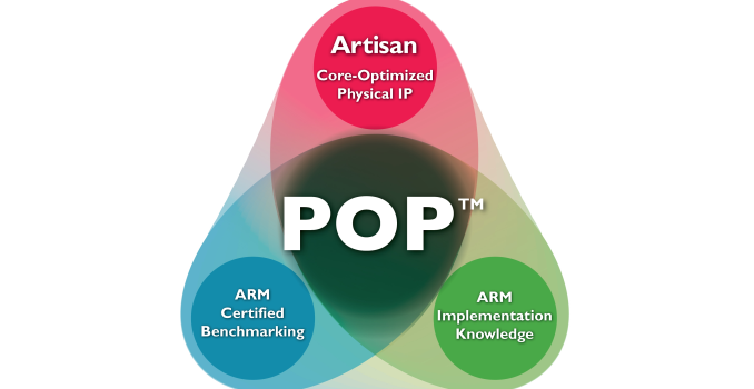
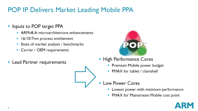
It’s here where ARM’s POP IP (Which by the way is not an acronym) comes into play: Roughly speaking, POP IP is a set of tools and resources that are created by ARM to accelerate and facilitate the implementation part of SoC development. This includes standard cell libraries, memory compilers, timing benchmarks, process optimized design changes and in general implementation knowledge that ARM is able to amass during the IP block development phase.

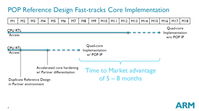
The main goal is to relieve the vendor from re-doing work that ARM has already done and thus enable a much better time-to-market compared to vendors which have their in-house implementation methodology (Samsung and Qualcomm, among others, for example). ARM explains this can give an up to 5-8 month time to market advantage which is critical in the fast-moving mobile SoC space.

One aspect that seemed to be misunderstood, and even myself had some unclear notions about, is that POP IP is not a hard-macro offering but rather all the resources that enable a vendor to achieve that hard-macro (GDSII implementation).

This is where we come back to today’s announcement. ARM’s new POP IP targets UMC’s new 28nm process called 28HPCfor ARM’s Cortex A7 and Cortex A53 cores. The acronym has a dual meaning standing for 28nm High Performance Compact “UMC” or “Ultra-Low IDDQ” with IDDQ being the leakage current which is being describes as being considerably lower than UMC’s first-generation 28nm HKMG process and able to give significant battery life improvements to devices. 

While ARM isn’t able to disclose which vendors use POP IP, they state that the main target is low-cost Asian market, which most likely means various Chinese vendors. According to S.C. Chien, vice president, corporate marketing, UMC:

“Multiple customers from a variety of applications have engaged with UMC to design their products on 28HPCU. Our collaboration with long-time partner ARM enables UMC to offer a comprehensive design platform with POP IP for two of the most efficient ARM processor cores.”

ARM Announces New 28nm POP IP For UMC Foundry

ARM Announces New 28nm POP IP For UMC Foundry

Today ARM announces a new POP IP offering directed at UMC’s new 28HPCmanufacturing process. To date we haven’t had the opportunity to properly explain what ARM’s POP IP actually is and how it enables vendors to achieve better implementation of ARM’s IP offerings. While for today’s pipeline announcement we’ll be just explaining the basics, we’re looking forward to a more in-depth article in the following months as to how vendors take various IPs through the different stages of development. 

When we talk about a vendor licensing an ARM IP (CPU for example), this generally means that they are taking the RTL (Register Transfer Level) design of an IP. The RTL is just a logical representation of the functioning of a block, and to get to from this form to one that can be implemented into actual silicon requires different development phases which is generally referred to as the physical implementation part of semiconductor development. 

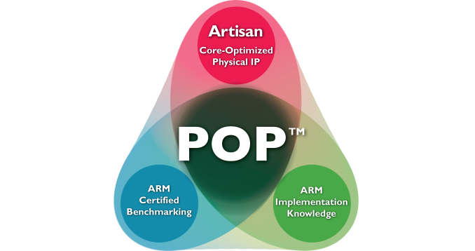
It’s here where ARM’s POP IP (Which by the way is not an acronym) comes into play: Roughly speaking, POP IP is a set of tools and resources that are created by ARM to accelerate and facilitate the implementation part of SoC development. This includes standard cell libraries, memory compilers, timing benchmarks, process optimized design changes and in general implementation knowledge that ARM is able to amass during the IP block development phase.

The main goal is to relieve the vendor from re-doing work that ARM has already done and thus enable a much better time-to-market compared to vendors which have their in-house implementation methodology (Samsung and Qualcomm, among others, for example). ARM explains this can give an up to 5-8 month time to market advantage which is critical in the fast-moving mobile SoC space.

One aspect that seemed to be misunderstood, and even myself had some unclear notions about, is that POP IP is not a hard-macro offering but rather all the resources that enable a vendor to achieve that hard-macro (GDSII implementation).

This is where we come back to today’s announcement. ARM’s new POP IP targets UMC’s new 28nm process called 28HPCfor ARM’s Cortex A7 and Cortex A53 cores. The acronym has a dual meaning standing for 28nm High Performance Compact “UMC” or “Ultra-Low IDDQ” with IDDQ being the leakage current which is being describes as being considerably lower than UMC’s first-generation 28nm HKMG process and able to give significant battery life improvements to devices. 

While ARM isn’t able to disclose which vendors use POP IP, they state that the main target is low-cost Asian market, which most likely means various Chinese vendors. According to S.C. Chien, vice president, corporate marketing, UMC:

“Multiple customers from a variety of applications have engaged with UMC to design their products on 28HPCU. Our collaboration with long-time partner ARM enables UMC to offer a comprehensive design platform with POP IP for two of the most efficient ARM processor cores.”

Ambarella CES 2016 Tour

Ambarella CES 2016 Tour

Yesterday Josh and I met with Ambarella and went on a tour of their exhibits. The main topic was their new line of SoCs, along with the various products and projects that have branched off from what these SoCs and their video encoding and decoding capabilities can enable.

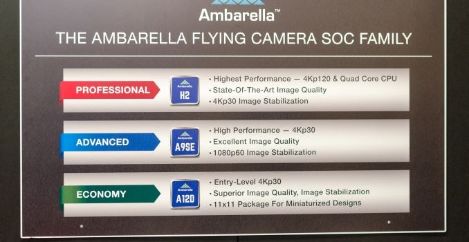
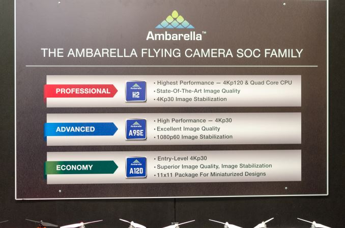
The high end SoC in Ambarella’s line of chips for cameras is H2. H2 is built on Samsung’s 14nm process, and it incorporates a quad core 1.2GHz Cortex A53 cluster, and its capable of encoding 4K HEVC video at 60fps, or 4K AVC video at 120fps. The latter makes it capable of doing 4K slow mo videos by playing back the 120fps footage at 30fps. H2 also includes support for capturing video with 10-bit color, as well as support for HDR which has recently been integrated into the Blu-ray and UHD standards.

The next SoC in Ambarella’s line is H12. H12 isn’t shown in the image above, but it’s capable of encoding 4Kp30 video using AVC or HEVC. It uses a single 1GHz Cortex A9 core, and it’s built on a 28nm process.

The last two SoCs are A9SE and A12D. A12D is an entry level chip, while A9SE has some advanced functionality, but is intended for devices sitting at lower prices than ones that incorporate H2. A9SE offers 4Kp30 support, and can do 1080p60 video with electronic image stabilization.

One of the demos that Ambarella showed was an example of their electronic image stabilization for 4K video. Part of the drive behind this is the fact that stabilization on drones has had to be implemented using a mechanical system that shifts the camera along each axis to keep the sensor in the same position. This type of system increases the size, mass, and cost of the drone, and so it’s obviously something that drone makers would be keen to eliminate in order to allow for reduced prices and improved battery life. Above you can see a short video which compares two real time video feeds with EIS on and off. As you can see, the difference is dramatic, and the level of stabilization that can be done by the SoC is extremely impressive.

Another exhibit showcased the ability to record 4Kp120 video. This is the first time that I’ve seen any 4K footage recorded at a high enough frame rate to slow it down an appreciable amount.

Several of the exhibits that Ambarella had related to technology that will be used in self driving cars. Some of this builds on demos that were shown at last year’s CES. The demo that I found most interesting is the electronic mirror. Essentially this is a mirror that integrates a display which streams footage from a rear-mounted camera on your car. The reasons for using an electronic mirror include the ability to have a higher field of view, no obstruction from passengers in rear seats, and better visibility at night due to the HDR processing that can be done by the SoC at night in order to make the car behind you visible without making the headlights overpoweringly bright. It’s important to note that the mirror can act as a normal mirror in conditions when the camera is not necessary.

Another car-related demo from Ambarella involved mapping the environment around a vehicle using cameras mounted on the various sides. This isn’t exactly a new concept, but it does tie in with their new SoCs. Some things demoed included environment mapping for self-driving cars, and using the cameras to view an environment in order to implement features like automatic parking.

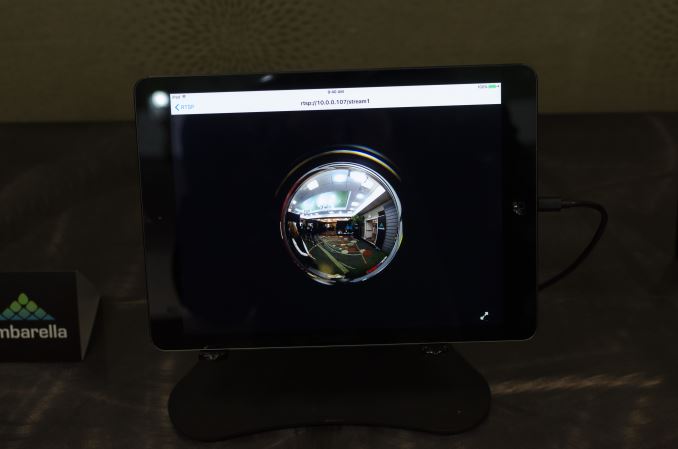
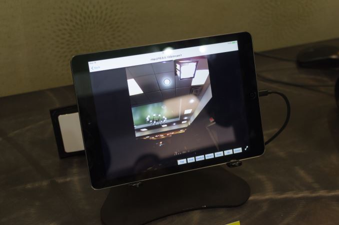
The last demo that I found quite interesting demonstrated the image de-warping capabilities of the H2 and H12 SoCs. The demonstration shown gave the example of a fisheye camera being used in a security camera mounted on on a door, with the de-warping being used to put the image into a state that is easy to view.

As far as real-time video encoding goes, the tech being shown off by Ambarella definitely impresses. I haven’t seen 4Kp120 recording in anything else that is consumer-focused, and the push for improved 4Kp60 HEVC encoding with 10-bit color and HDR support is something that will be necessary as new standards for UltraHD video are adopted.