Mobile


BaseMark Announces The Power Assessment Tool (PAT)

BaseMark Announces The Power Assessment Tool (PAT)

Basemark has traditionally been a software company. We’ve seen and used a lot of their benchmarking test suites including Basemark OS and Basemark X. Seeking to expand its portfolio by not only providing software benchmarks to quantify performance of devices, Basemark looks to provide hardware to enable users to measure power-consumption and power-efficiency of devices. Here is where the PAT (Power Assessment Tool) comes in. The PAT is a tool that doesn’t require destructive dismantlement of a device to be able to measure its power consumption. This is an area where I’m particularly familiar with as over the last year and more have been instrumenting a lot of smartphones via external power supplies and measurement equipment by physically opening them and replacing the lithium power cells. 

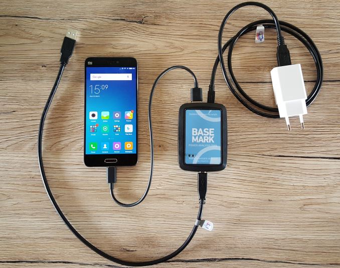
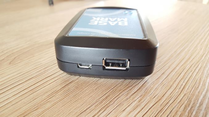
Basemark relies on the fact that when smartphones are fully charged, they usually enter a power bypass-mode where the internal battery cell is no longer used, and power is instead drawn directly from the connected charger. To do this the PAT is connected to a conventional charger input. Currently this is a microUSB port but Basemark tells me future revisions might consider going USB C. The output is a USB-A port and thus one can connect any kind of receiving device, be it USB C, microUSB or Lightning port. 

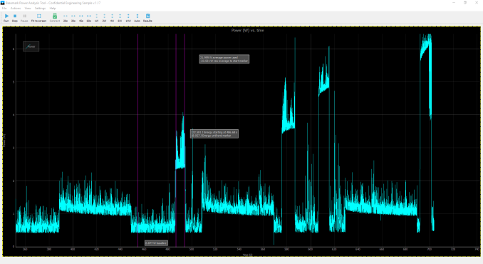
On the software-side the PAT comes with an interface and analysis software that is able to connect to the hardware and show in real-time the power consumption of the device. 

It’s still a bit early to talk about the capabilities of the beta software but Basemark shows promise and once all features are implemented the PAT should represent great value in terms of analysis for both professionals and enthusiastic hobbyists.

The charger input power measurement methodology does come with limitations. For example power consumption exceeding charger power will lead to the device PMIC to compensate by drawing power from the battery – power which then can no longer be tracked. Another problematic scenario is when devices implement charge current limits when the screen is on. While in practice they would be able to charge at rates of up to 12W, they limit themselves to ~5W when the device is used. This limit sometimes falls below the peak power consumption of devices and thus can result in a misleading measurement data. 

While the PAT is officially advertised and validated for power measurement over a device’s USB port, an interesting use-case that I couldn’t help myself testing is trying to use it to directly power and measure the device’s battery power input. With some cable splicing and modifications to be able to just use the + and GND pins of the USB connectors and connect them to the device’s battery input I was able to avoid any of the limitations and draw-backs of measuring power via the device’s input power.

Basemark publishes that the power range on the input and output ports ranges from 4.10V (3.9V output) to 5.25V at up to 1.8A. I’m not sure if these are technical limits or simply the currently validated ranges that Basemark has tested the hardware on as I had no issues connecting fast-chargers with supply voltages of up to 9V. The internal ADC is 16-bit in resolution and able to measure voltage with accuracy of ÷ 140 µV and currents at up to ÷ 1 mA accuracy for the least-significant-bit (LSB). Currently the data sample-rate is configurable down to 1ms resolution but Basemark tells me that the internal ADC is capable of up to ~100kS/s and maybe taken advantage of in future firmware updates.

Overall the PAT is an interesting and useful little tool. Basemark prices the first generation at 995€ without VAT for corporate costumers with limited availability starting in April. At a rather steep starting price, the PAT will need to distinguish itself via its software and analysis capabilities. I’ll be reviewing the PAT more in-depth in the coming months as Basemark continues to refine the software suite, so keep an eye out for more in-depth testing!

MWC 2016: Hands On with Alcatel’s Plus 10, A Win10 2-in-1

MWC 2016: Hands On with Alcatel’s Plus 10, A Win10 2-in-1

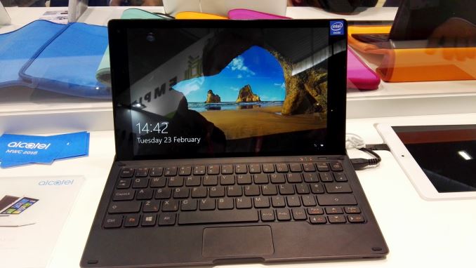
Ever since OLPC tried to bring cheaper portable laptops around the world, there has been a steady stream of low level devices with one primary goal – get users online at a low price point. So while Mobile World Congress has been talking a lot about super high end devices and smartphones, alongside Alcatel’s launch of the Idol 4 and Idol 4S they are also launching the Plus 10, a new Windows 10 2-in-1 tablet.

The tablet houses the hardware – within the 10.1-inch IPS panel running at a 1280×800 resolution there is an Intel Atom x5-Z8350 SoC (quad core 14nm Cherry Trail, 1.92 GHz) with integrated HD 400 Graphics (12 EUs, 500 MHz), 2GB of DRAM, 32GB of internal storage which can be expanded via a 64GB microSD card, and a 5830 mAh battery. The tablet has some minor IO: USB, micro-USB and micro-HDMI, but the keyboard gets a full-sized USB Type-A and a couple of other ports. The keyboard also adds another 2590 mAh battery, but the whole unit is Cat 4 LTE capable, supporting up to 150 Mbps, and the keyboard can act as a mobile hotspot for up to 15 users.


Sim Card Slot

We were able to get some hands on time with the device, and despite the fact that none of the keyboards seemed to work when installed, it came across as an easy to use tablet. Obviously touch on Windows isn’t the best experience without dedicated software, but the screen seemed bright enough when head-on and if the keyboard worked it could make an easy working experience. Because the device is a 2-in-1, the tablet and keyboard detach – the tablet can face either direction, making it easy for the keyboard to face away and act as a stand.

Another issue was when closing the tablet into the keyboard – because of the rigid lip on the keyboard end where the two connected, there wasn’t a good connection. Andrei pointed out that one magnet was weak (perhaps it was a demo model) but it went beyond that, it was clear that the two parts didn’t even line up, and I doubt they would stay together when being carried like a 2-in-1 is normally carried.

One thing worth noting in our examination is the use of 32-bit Windows 10. This might go some way of explaining the 2GB DRAM installed (most likely single channel as well), but might have repercussions for software compatibility and performance. The Wi-Fi module wasn’t listed in the official press release, but we found it listed in the system manager as the Realtek RTL8723BS, which is an 802.11n part which is limited to single stream 1T1R 2.4 GHz operation, making it a very cheap option to use.

We were told that the device will retail for around 259-269 Euros, which makes it a sizable and interesting upgrade from something like the HP Stream 11 series of clamshell devices, albeit with a few obvious flaws (at least on these units). I have a feeling these might end up in an educational context as one of the primary markets, alongside sales to end-users.

ARM Announces Cortex-A32 IoT and Embedded Processor

ARM Announces Cortex-A32 IoT and Embedded Processor

Today ARM announces the new Cortex A32 ultra-low power/high efficiency processor IP. For some readers this might come as a surprise as it’s only been a few months since we saw the announcement of the Cortex A35 which was presented as a replacement for the Cortex A7 and A5, so this leaves us with the question of where the Cortex A32 positions itself against both past IPs such as the A7 and A5, but also how it compares against the A35.

The answer is rather simple: It’s still a replacement for the A7 and A5, but targets even lower power use-cases than what the A35 was designed for. While ARM sees the A35 as the core for the next billion low-end smartphones, the A32 seems to be more targeted at the embedded market. In particular it’s the “Rich Embedded” market that ARM seems to be excited about. The differentiation lies between use-cases which require a full-fledged MMU and thus able to run full operating systems based on Linux, and those who don’t and could make due with a simpler micro-controller based on one of ARM’s Cortex-M profile IPs. It’s also worth to mention that although last time we claimed that the A35 would servce the IoT market, ARM seems to see wearables and similar devices as part of the “Rich Embedded” umbrella-term and thus now it seems more likely that it’s the A32 that will be the core that will power such designs.

This leads us to the mystery of what exactly is the A32? During the briefing the only logical question that seemed to come to mind is: “Is this an A35 with 64-bit ‘slashed off‘?” While ARM chuckled at my oversimplification, they agreed that from a very high-level perspective that it could be considered as an accurate description of the A32.

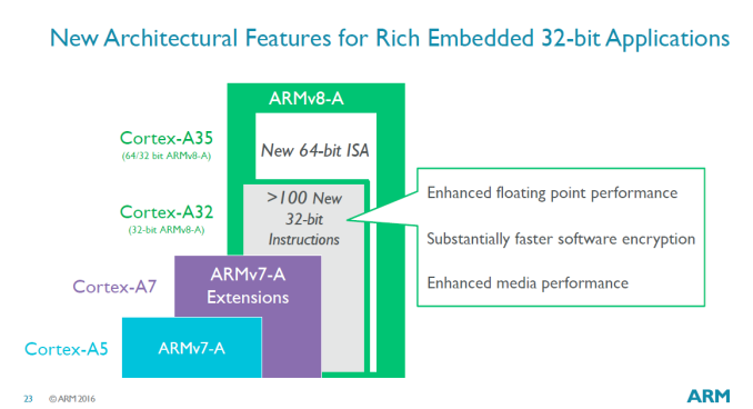
In more technical terms, the A32 is an 32-bit ARMv8-A processor with largely the same microarchitectural characteristics of the Cortex A35. As a reminder to our readers out there: The ARMv8 ISA is not only an 64-bit instruction set but also contains many improvements and additions to the 32-bit profile commonly named as AArch32. Among the larger differences between the A35 and A32 is that the latter’s microarchitecture has been tuned and optimized to achieve the best performance and efficiency for 32-bit.

Indeed, performance wise, the A32 is advertised as being able to match the Cortex A35.  The improvements lie in power efficiency: as a result of dropping its 64-bit capabilities, the new core is now able to achieve up to 10% better efficiency than the Cortex A35. Similarly to the A35, the A32 promises to achieve vastly superior performance per clock versus the Cortex A5 and A7, achieving anywhere from a 31% increase in integer workloads to a massive factor of 13x in crypto workloads, which the A32 is still capable of as they’re included in the AArch32 ARMv8 profile.

While only a few months ago the Cortex A35 was advertised as ARM’s smallest Cortex-A core, this title has now been passed on to the A32. ARM claims the core is around 30% smaller than the A35; The decrease in size, mostly due to the slimming down of the micro-architecture due the removal of 64-bit capability, allows the Cortex A32 to scale down to <0.25mm² in its smallest configuration, a significant decrease compared to the A35’s disclosed <0.4mm². The core remains as configurable as the Cortex A35, able to run as either as single core or any as a cluster up to four cores. Optionally vendors can also configure cache sizes, with L1 ranging from 8KB to 32KB and L2 either being completely absent to up to 1MB in size.

ARM’s philosophy of “having the right design for the job” now seems more apparent than ever as we see an steadily increasing portfolio of processor IPs specialized for different use-cases. The A32 seems to fit right in with this strategy and we’ll more than certainly see a large array of devices powered by the core in the future to come.

ARM Announces Cortex-A32 IoT and Embedded Processor

ARM Announces Cortex-A32 IoT and Embedded Processor

Today ARM announces the new Cortex A32 ultra-low power/high efficiency processor IP. For some readers this might come as a surprise as it’s only been a few months since we saw the announcement of the Cortex A35 which was presented as a replacement for the Cortex A7 and A5, so this leaves us with the question of where the Cortex A32 positions itself against both past IPs such as the A7 and A5, but also how it compares against the A35.

The answer is rather simple: It’s still a replacement for the A7 and A5, but targets even lower power use-cases than what the A35 was designed for. While ARM sees the A35 as the core for the next billion low-end smartphones, the A32 seems to be more targeted at the embedded market. In particular it’s the “Rich Embedded” market that ARM seems to be excited about. The differentiation lies between use-cases which require a full-fledged MMU and thus able to run full operating systems based on Linux, and those who don’t and could make due with a simpler micro-controller based on one of ARM’s Cortex-M profile IPs. It’s also worth to mention that although last time we claimed that the A35 would servce the IoT market, ARM seems to see wearables and similar devices as part of the “Rich Embedded” umbrella-term and thus now it seems more likely that it’s the A32 that will be the core that will power such designs.

This leads us to the mystery of what exactly is the A32? During the briefing the only logical question that seemed to come to mind is: “Is this an A35 with 64-bit ‘slashed off‘?” While ARM chuckled at my oversimplification, they agreed that from a very high-level perspective that it could be considered as an accurate description of the A32.

In more technical terms, the A32 is an 32-bit ARMv8-A processor with largely the same microarchitectural characteristics of the Cortex A35. As a reminder to our readers out there: The ARMv8 ISA is not only an 64-bit instruction set but also contains many improvements and additions to the 32-bit profile commonly named as AArch32. Among the larger differences between the A35 and A32 is that the latter’s microarchitecture has been tuned and optimized to achieve the best performance and efficiency for 32-bit.

Indeed, performance wise, the A32 is advertised as being able to match the Cortex A35.  The improvements lie in power efficiency: as a result of dropping its 64-bit capabilities, the new core is now able to achieve up to 10% better efficiency than the Cortex A35. Similarly to the A35, the A32 promises to achieve vastly superior performance per clock versus the Cortex A5 and A7, achieving anywhere from a 31% increase in integer workloads to a massive factor of 13x in crypto workloads, which the A32 is still capable of as they’re included in the AArch32 ARMv8 profile.

While only a few months ago the Cortex A35 was advertised as ARM’s smallest Cortex-A core, this title has now been passed on to the A32. ARM claims the core is around 30% smaller than the A35; The decrease in size, mostly due to the slimming down of the micro-architecture due the removal of 64-bit capability, allows the Cortex A32 to scale down to <0.25mm² in its smallest configuration, a significant decrease compared to the A35’s disclosed <0.4mm². The core remains as configurable as the Cortex A35, able to run as either as single core or any as a cluster up to four cores. Optionally vendors can also configure cache sizes, with L1 ranging from 8KB to 32KB and L2 either being completely absent to up to 1MB in size.

ARM’s philosophy of “having the right design for the job” now seems more apparent than ever as we see an steadily increasing portfolio of processor IPs specialized for different use-cases. The A32 seems to fit right in with this strategy and we’ll more than certainly see a large array of devices powered by the core in the future to come.

Samsung Announces the Gear 360: Consumer VR Content Creation

Samsung Announces the Gear 360: Consumer VR Content Creation

In addition to the Galaxy S7 and Galaxy S7 edge, Samsung is also announcing a camera for VR content. Rather than the extreme setups that we see with some of the current players in this space, Samsung is focusing on bringing VR content creation to the masses with the Gear 360.

In essence, the Gear 360 is a sphere slightly smaller than a tennis ball that can capture video and images from every angle around it with the use of two wide-angle f/2.0 15MP cameras to produce a 30MP image for stills, or 3840×1920 video. The Gear 360 has a 1350 mAh removable battery and microSD, a standard tripod mount, basic dust and splash resistance, and can pair to Galaxy smartphones with NFC and transfer data using WiFi Direct.

A companion app on Galaxy smartphones also allows for live preview of the footage, in addition to remote settings, transfer, and editing. For control of the device without a compatible smartphone, the Gear 360 has a 72×32 0.5″ PMOLED display and some rudimentary buttons to control its settings.

Finally, Samsung has stated that the Gear 360 will be available starting Q2 2016.