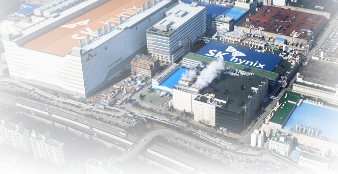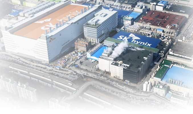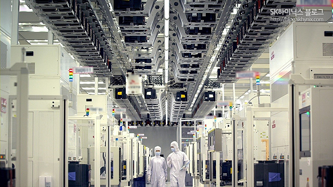
SK Hynix on Thursday announced plans to build a new manufacturing facility to produce NAND flash memory in South Korea, and also upgrade its DRAM production plant in China in a bid to sustain its production capacities. Both projects will initially cost SK Hynix about $2.6 billion (₩3.15 trillion) and are expected to be completed in 2019-2020. Over that time, the company will also invest additional money in the expansion of DRAM and NAND production in South Korea.
The new fab will be located in Cheongju, South Korea, not far from the company’s existing M8, M11 and M12 manufacturing facilities. SK Hynix intends to start the design of the new fab in January and begin construction of the shell and the cleanroom space in August. The company hopes to complete the building in June 2019, and by then finalize decisions regarding equipment installation based on market conditions. If everything proceeds as planned, the new fab will process the first wafers already in late 2019 and will make a sizeable contribution to SK Hynix’s revenue by late 2020. SK Hynix intends to spend $2.08 billion (₩2.2 trillion) on construction alone (a little lower than the manufacturer spent on the building for its massive flagship M14 plant) and then will have to invest in production tools.
SK Hynix does not reveal details about production capacity of the upcoming fab and does not share the area of its cleanroom space. However, judging by the investment in the building itself, the memory producer is set to build another giant manufacturing facility. Today, SK Hynix processes around 300 thousand DRAM wafers (300mm) and 230 thousand NAND flash wafers (also 300mm) at its different fabs every month. A significant portion of SK Hynix’s memory is made at its M14 fab, which monthly output (used to make both DRAM and NAND) is getting closer to a target of 200 thousand wafer starts per month, but is not there yet. The new fab will further increase 300-mm production capacities owned by SK Hynix.
| Overview of SK Hynix Manufacturing Capacities |
| |
Icheon, South Korea |
Cheongju, South Korea |
Wuxi, China |
| M14 |
M10 |
M8 |
M11 |
M12 |
Future |
C2 |
Maximum
Production Capacity
(300-mm wafer starts per month) |
<200K now
300K after upgrades |
130K |
– |
50K |
40K |
TBD |
130K |
| Application |
DRAM |
Yes |
Yes |
– |
Yes |
Yes |
Yes |
Yes |
| NAND |
2D + 3D |
2D + 3D |
– |
2D |
2D |
3D |
2D |
| DDIC |
– |
– |
Yes |
– |
– |
– |
– |
| PMIC |
– |
– |
Yes |
– |
– |
– |
– |
| CIS |
– |
Yes |
Yes |
– |
– |
– |
– |
| Wafer Size (mm) |
300 |
200 |
300 |
| 2016 Q3 |
| Total DRAM Output Today (300-mm wafer starts per month) |
300K |
| Total NAND Ouput Today (300-mm wafer starts per month) |
230K |
At present, SK Hynix plans to use the new fab to manufacture only 3D NAND flash memory, but once it is ready, the company will use it according to market demands and will be able to produce both NAND and DRAM at the same production facility. However, the flexibility of semiconductor fabs going forward will be more constrained. Traditionally manufacturers used similar step-and-scan lithography systems from companies like ASML or Nikon to produce both DRAM and 2D NAND. While production of the two types of memory has many differences, it was possible to balance a fab’s output depending on market conditions. Meanwhile, the industry (and SK Hynix) is transiting to 3D NAND and its production relies not only on lithography but also (mostly) on deposition and etching. 3D NAND manufacturing requires chemical vapor deposition (CVD) machines and high aspect ratio etch tools in addition to traditional step-and-scan systems. Once installed, CVD and etching equipment take precious cleanroom space and thus fewer scanners can be installed there. As a result, switching a production line from 3D NAND to DRAM and vice-versa gets more complicated since different equipment has to be installed. On the other hand, the upper floor of SK Hynix’s M14 fab is set to be used for 3D NAND production starting from 2017, which means that it is possible to make DRAM and 3D NAND in the same building.

As NAND flash is moving into three-dimensional space, planar DRAM will keep evolving for a long time (nonetheless, architectures like HBM and other types of 3D DRAM are developing as well) and will require new manufacturing technologies. As fabrication processes get thinner, DRAM makers have to increase the use of multi-patterning techniques, which makes production cycles longer and effectively lowers output of fabs. In a bid to maintain its DRAM production capacities (and ultimately preserve its market share), SK Hynix plans to expand cleanroom space of its C2 fab in Wuxi, China, to install additional step-and-scan systems. The upgrade of the plant will cost SK Hynix approximately $790.68 million (₩950 billion). The company will start the work in July next year and plans to complete them in April 2019. The manufacturer does not disclose output of the production facility officially, but analysts from TrendForce believe that it represents roughly half of SK Hynix’s DRAM output and can process up to 130 thousand wafers (300mm) per month.
In the recent years, SK Hynix announced major plans to expand its existing semiconductor manufacturing capacities and build new ones. In total, the company intends to spend $38.28 billion (₩46 trillion) on fabs in the mid and long-term future, which is a serious commitment to the semiconductor industry in general.
Related Reading:

