GPUs


NVIDIA Releases 372.70 WHQL Game Ready Driver

NVIDIA Releases 372.70 WHQL Game Ready Driver

It’s driver update time again. This time with a small list of fixes and a relatively large list of game ready titles. Though the list is a bit inflated with Deus Ex: Mankind divided sitting in a second time and Quantum break not seeing release for two more weeks, luck and users favor the prepared.

With this driver update continuing 370 driver branch, we start with a short list of fixes including issues in Windows 7 through 10 with Fallout 4 where enabling SSAO instead of HBAO+ would cause your Pipboy to go black and unreadable. Another issue resolved is high deferred Procedure Call latency in driver version 368.69 when upgrading to a GeForce GTX 1080, and the last fix listed only under Windows 10 was video corruption found when certain standard definition videos were up-scaled to full screen after a driver update.

The big reason most will be interested in this driver are the game ready updates. Key among these is World of Warcraft: Legion, the 6th and latest Expansion to what’s still the most popular MMORPG out there. Following WoW: Legion we have the Battlefield 1 open beta starting, and NVIDIA has made sure that their GPU’s are ready as part of this week’s driver update. Meanwhile, Quantum Break, which saw release earlier this year on both the Xbox One and the Windows 10 store as a DX12 title, will be released on Steam with DX11 support, allowing more people to enjoy the game. Steam currently lists the release date as September 14th, making NVIDIA ready a head of the games (re) release. Lastly, Deus Ex: Mankind Divided is listed again under game ready this week. While I’m unsure of why it’s game ready again, NVIDIA does state in the release notes that Deus Ex’s 3D Vision profile has been upgraded from fair to excellent, for those still sporting the specs (read: spectacles) to play in 3D.

Anyone interested can download the updated drivers through GeForce Experience or on the NVIDIA driver download page. More information on this update and further issues can be found in the 372.70 release notes.

NVIDIA Announces Paragon Game Bundle For GeForce Video Cards

NVIDIA Announces Paragon Game Bundle For GeForce Video Cards

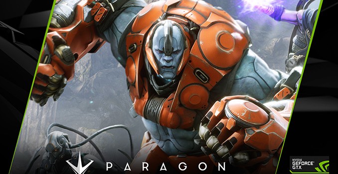
As game releases ramp up and GPU manufacturers build market interest approaching the fall season, bundles seem to be popping up like daisies. The latest to join the fray is NVIDIA’s Paragon Game Ready Pack.

Paragon is the latest game out of E…

NVIDIA Announces Paragon Game Bundle For GeForce Video Cards

NVIDIA Announces Paragon Game Bundle For GeForce Video Cards

As game releases ramp up and GPU manufacturers build market interest approaching the fall season, bundles seem to be popping up like daisies. The latest to join the fray is NVIDIA’s Paragon Game Ready Pack.

Paragon is the latest game out of E…

Hot Chips 2016: NVIDIA Pascal GP100 Die Shot Released

Hot Chips 2016: NVIDIA Pascal GP100 Die Shot Released

The first day of conference sessions wrapped up earlier this evening at the annual Hot Chips symposium. One of the computing industry’s lower-key events, the IEEE conference for high performance chips is not a venue for product announcements, but instead a more focused conference for tech companies and their engineers to let their hair down a bit and present some deeper technical workings of their products. Even these aren’t full product briefings – since they’re often for future products – but it’s a good venue to dive a little deeper and learn a little bit more about the technologies and decisions that have gone into putting these chips together.

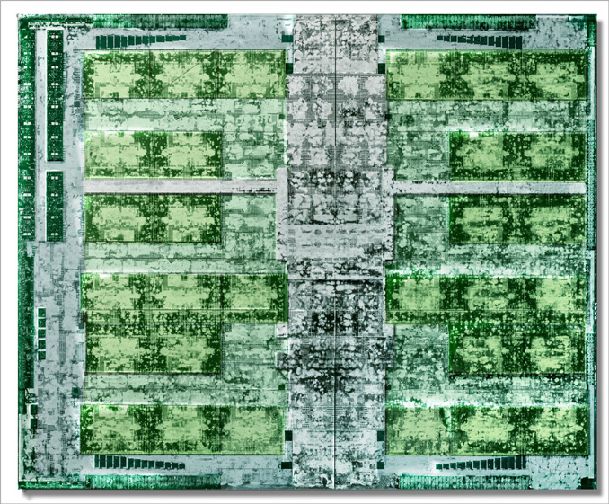
Over the next two days we’ll be covering the highlights of several presentations, but I wanted to start this year’s coverage off with some nerdy pictures. I am of course referring to die shots, as NVIDIA has released the first die shot of their behemoth 610mm2 GP100 die as part of a presentation on Pascal and NVLink 1.0. Die shots have been relatively rare in the GPU industry in recent years, particularly those for the highest-end GPUs with the most features.

GP100 is particularly interesting because it’s the first NVIDIA part featuring HBM and NVLink, two interfaces which (at least for NVIDIA) premiered on GP100. The die shot itself is not significantly enhanced (and I’m not going to spoil a good die shot here), but even with just basic coloring you can make out features such as the thread scheduler and other uncore features in the center, along of course with the SMs. GP100, as a reminder, has 60 in all, organized into 30 TPCs, the latter of which is what you’re probably counting right now.

Top and bottom of this picture appear to be the HBM2 interfaces. Despite the width of GP100’s 4096-bit HBM2 bus, the space consumed by HBM2 appears to be relatively small on the admittedly large GPU, which is one of the benefits of HBM as it allows for very tight routing and simpler GPU-side logic. Going HBM didn’t just get NVIDIA more memory bandwidth, but I fully expect it also got them a meaningful increase in die area that they could dedicate to GPU logic.

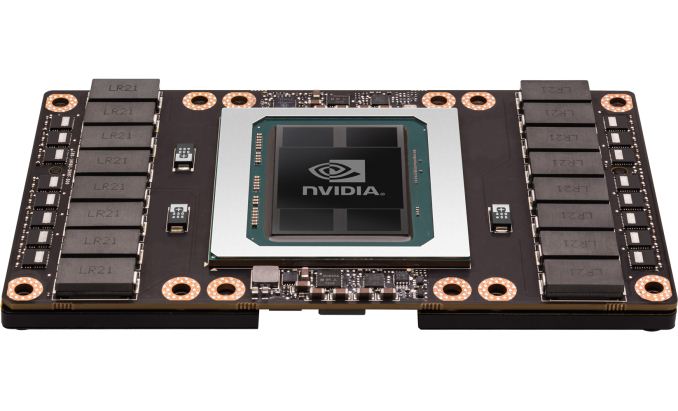
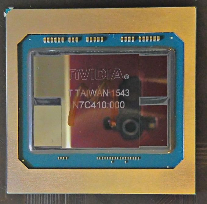
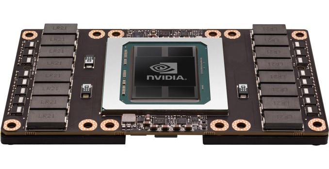
Meanwhile the presentation also gives us our best shot to date of a full (and presumably production) GP100 package. Note the tight spacing between the HBM2 stacks and the GPU die; NVIDIA did not waste any space here, as the memory stacks have been placed as close as they can be. Both the memory and GPU sit on top of the silicon interposer, itself not much larger than the hardware it sits on. Due to the large size of GP100, every millimeter ends up mattering here, as the resulting interposer has to be quite large even with this dense packing. This also does a great job illustrating just how much larger HBM2 stacks are than HBM1 stacks, as they now are a considerable fraction of the die size of GP100 itself, as opposed to the smaller HBM1 stacks used on AMD’s Fury X last year.

The big question, of course, is when this technology will trickle down into cheaper, consumer-level boards. Right now HBM2 is still quite expensive, while GDDR5X has allowed NVIDIA to cover much of their bandwidth needs on consumer parts with the cheaper memory technology. However as we’ll see in the Hot Chips memory presentation, Samsung and Xilinx have some ideas on how to handle that…

Hot Chips 2016: NVIDIA Pascal GP100 Die Shot Released

Hot Chips 2016: NVIDIA Pascal GP100 Die Shot Released

The first day of conference sessions wrapped up earlier this evening at the annual Hot Chips symposium. One of the computing industry’s lower-key events, the IEEE conference for high performance chips is not a venue for product announcements, but instead a more focused conference for tech companies and their engineers to let their hair down a bit and present some deeper technical workings of their products. Even these aren’t full product briefings – since they’re often for future products – but it’s a good venue to dive a little deeper and learn a little bit more about the technologies and decisions that have gone into putting these chips together.

Over the next two days we’ll be covering the highlights of several presentations, but I wanted to start this year’s coverage off with some nerdy pictures. I am of course referring to die shots, as NVIDIA has released the first die shot of their behemoth 610mm2 GP100 die as part of a presentation on Pascal and NVLink 1.0. Die shots have been relatively rare in the GPU industry in recent years, particularly those for the highest-end GPUs with the most features.

GP100 is particularly interesting because it’s the first NVIDIA part featuring HBM and NVLink, two interfaces which (at least for NVIDIA) premiered on GP100. The die shot itself is not significantly enhanced (and I’m not going to spoil a good die shot here), but even with just basic coloring you can make out features such as the thread scheduler and other uncore features in the center, along of course with the SMs. GP100, as a reminder, has 60 in all, organized into 30 TPCs, the latter of which is what you’re probably counting right now.

Top and bottom of this picture appear to be the HBM2 interfaces. Despite the width of GP100’s 4096-bit HBM2 bus, the space consumed by HBM2 appears to be relatively small on the admittedly large GPU, which is one of the benefits of HBM as it allows for very tight routing and simpler GPU-side logic. Going HBM didn’t just get NVIDIA more memory bandwidth, but I fully expect it also got them a meaningful increase in die area that they could dedicate to GPU logic.

Meanwhile the presentation also gives us our best shot to date of a full (and presumably production) GP100 package. Note the tight spacing between the HBM2 stacks and the GPU die; NVIDIA did not waste any space here, as the memory stacks have been placed as close as they can be. Both the memory and GPU sit on top of the silicon interposer, itself not much larger than the hardware it sits on. Due to the large size of GP100, every millimeter ends up mattering here, as the resulting interposer has to be quite large even with this dense packing. This also does a great job illustrating just how much larger HBM2 stacks are than HBM1 stacks, as they now are a considerable fraction of the die size of GP100 itself, as opposed to the smaller HBM1 stacks used on AMD’s Fury X last year.

The big question, of course, is when this technology will trickle down into cheaper, consumer-level boards. Right now HBM2 is still quite expensive, while GDDR5X has allowed NVIDIA to cover much of their bandwidth needs on consumer parts with the cheaper memory technology. However as we’ll see in the Hot Chips memory presentation, Samsung and Xilinx have some ideas on how to handle that…