Analyzing Apple’s A8 SoC: PowerVR GX6650 & More
With their iPhone keynote behind them, Apple has begun updating some of their developer documentation for iOS to account for the new phone. This of course is always a fun time for tech punditry, as those updates will often include information on the hardware differences in the platform, and explain to developers the various features that different generations of hardware can offer developers.
To that end we have compiled a short analysis of the A8 SoC based on these documents and other sources. And we believe that at this point we have a solid idea of the configuration of Apple’s latest SoC.
| Apple SoC Specifications | ||||||
| Apple A6 | Apple A7 | Apple A8 | ||||
| CPU | Swift @ 1.3GHz(x2) | Cyclone @ 1.3GHz (x2) | Enhanced Cyclone @ 1.4GHz (x2)? | |||
| GPU | PVR SGX543MP3 | PVR G6430 | PVR GX6650 | |||
| RAM | 1GB LPDDR2 | 1GB LPDDR3 | 1GB LPDDR3? | |||
A8’s GPU: Imagination PowerVR Series6XT GX6650
On the GPU front this year appears to be especially bountiful. After being tipped to an update for Apple’s Metal Programming Guide, we can now infer with near certainty that we know what the A8 GPU is.
New to this edition of the Metal Programming Guide is a so-called iOS_GPUFamily2, which joins the existing iOS_GPUFamily1. We already know that the iOS_GPUFamily1 is based around Imagination’s PowerVR Series 6 G6430 GPU, so the real question is what does iOS_GPUFamily2 do that requires a separate family? The answer as it turns out is ASTC, the next generation texture compression format is being adopted by GPU vendors over the next year or so.
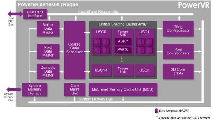
Imagination’s PowerVR Series6 family of GPUs predates ASTC and as a result iOS_GPUFamily1 does not support it. However we know that Imagination added support for it in their Series6XT designs, which were announced at CES 2014. Coupled with the fact that Apple’s documentation supports the idea that all of their GPUs are still TDBR (and thus PowerVR), this means that the GPU in the A8 must be a Series6XT GPU in order for ASTC support to be present.
This leaves the question of which of Imagination’s 4 Series6XT Apple is using. Imagination offers a pair of 2 core designs, a 4 core design (GX6450), and a 6 core design (GX6650). Considering that Apple was already using a 4 core design in A7, we can safely rule out the 2 core designs. That leaves us with GX6450 and GX6650, and to further select between those options we turn to Apple’s A8 performance estimates.
| Apple SoC Evolution | |||||
| CPU Perf | GPU Perf | Die Size | Transistors | Process | |
| A5 | ~13x | ~20x | 122m2 | <1B | 45nm |
| A6 | ~26x | ~34x | 97mm2 | <1B | 32nm |
| A7 | 40x | 56x | 102mm2 | >1B | 28nm |
| A8 | 50x | 84x | 89mm2 | ~2B | 20nm |
A8 is said to offer 84x the GPU performance of the iPhone 1, while last year Apple stated that the A7 offered 56x the iPhone 1’s performance. As a result we can accurately infer that the A8 must be 1.5x faster than the A7, a nice round number that makes it easier to determine with GPU Apple is using. Given Apple’s conservative stance on clockspeeds for power purposes and the die space gains from the 20nm process, accounting for a 50% performance upgrade is easily done by replacing a 4 core G6430 with the 6 core GX6650. At equal clockspeeds the GX6650 should be 50% faster on paper (matching Apple’s paper numbers), leading us to strongly believe that the A8 is utilizing a PowerVR Series6XT GX6650 GPU.
Once the iPhone 6 is out and Chipworks can photograph the SoC, this should be easy to confirm. If Apple is using a GX6650 then the die size of the GPU portion of the A8 should be very similar to the die size of the GPU portion of the A7. Otherwise if it is the 4 core GX6450, then Apple should see significant die size savings from using a 20nm fabrication process.
A8’s CPU: A Tweaked Cyclone?
Though we typically avoid rumors and leaks due to their high unreliability, after today’s presentation by Apple we have just enough information on A8’s CPU performance to go through the leak pile and start picking at leak. From that pile there is one leak in particular that catches our eye due to the fact that it matches Apple’s own statements.
On Monday night a supposed Geekbench 3 score of the iPhone 6 was posted. In this leak the iPhone 6 was listed as having a single-core score of 1633 points and a multi-core score of 2920 points. Curiously, these values are almost exactly 25% greater than the Geekbench 3 scores for the iPhone 5S (A7), which are 1305 points and 2347 points respectively.
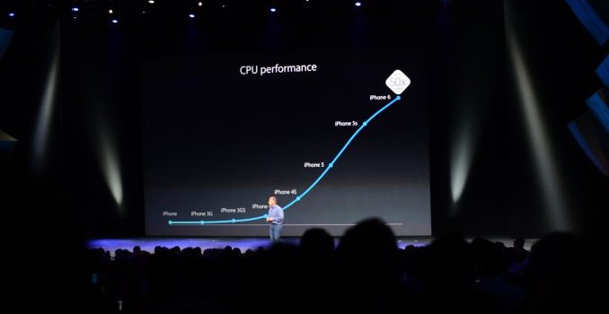
The fact that ties all of this data together is that in their iPhone 6 presentation, Apple informed viewers that the iPhone 6 is 25% faster than the iPhone 5S. This data was later backed up with their latest CPU performance graph, which put the iPhone 6 at a score of 50x versus a score of 40x for the iPhone 5S.
Given Apple’s data, it looks increasingly likely that the leaked Geekbench 3 results for the iPhone 6 are in fact legitimate. The data leaked matches Apple’s own performance estimates, and in fact does so very well.
In which case we can infer a couple of points about the A8’s CPU, starting with the clockspeed. Given no other reason to doubt this data at the moment and given Apple’s preference for low clocked SoCs, the 1.4GHz reading appears legitimate. In which case this would be a 100MHz increase over the 1.3GHz A7 found in the iPhone 5S.
However the fact that it’s a 100MHz increase also means that clockspeeds alone cannot account for the full 25% performance gain that Apple is promoting and that these Geekbench results are reporting, as 1.4GHz is only a roughly 8% clockspeed increase over 1.3GHz. This in turn means that there must be more going on under the hood to improve the A8’s CPU performance other than clockspeed alone, which rules out a straight-up reuse of Apple’s Cyclone CPU.
Since Apple already had a solid ARMv8 architecture with Cyclone, there’s no reason to believe that they have thrown out Cyclone so soon. However this does strongly suggest that Apple has made some unknown revisions to Cyclone to further boost its single-threaded (Instruction Level Parallelism) performance. What those tweaks are remain to be seen as we would need to be able to benchmark the A8 in depth to even try to determine what Apple has changed, but for the moment it looks like we’re looking at an enhanced or otherwise significantly optimized version of Cyclone. And given Apple’s already high ILP, squeezing out another 16% or so would be a significant accomplishment at this time, especially for only a year’s turnaround.
1GB of RAM
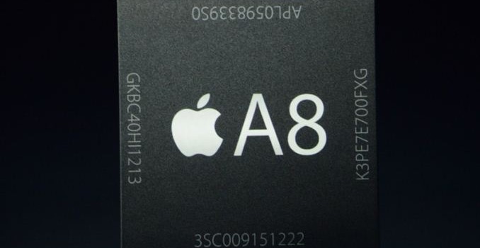
Last but not least, the apparent validity of the Geekbench 3 leak means that one last piece of information on the A8 can apparently be confirmed: the earlier rumors about it being paired with 1GB of RAM are true. Unfortunately Apple’s official product image of the A8 is of no help here – it’s clearly a doctored version of the A7 image based on the product numbers attached – but this information is consistentwith earlier rumors based on leaked images of the real A8, which had also suggested the SoC contained 1GB of RAM. Again this is based on what we believe is a sound assumption that the Geekbench 3 leak is accurate since it so closely matches Apple’s own CPU performance estimates, but at this point we don’t have any substantial reason to doubt the data.

Image Courtesy Macrumors
The good news is that this is going to be the easiest aspect of the iPhone 6 to confirm, since diagnostic apps will be able to query the phone for the RAM amount. So one way or another we should know for sure come September 19th.

