CPUs


Intel Introduces New Braswell Stepping with J3060, J3160 and J3710

Intel Introduces New Braswell Stepping with J3060, J3160 and J3710

When a processor is manufactured, it has a series of designations to identify it, such as the name. But alongside this, as with almost every manufactured product ever, each product will go through a number of revisions and design reinventions to do the same thing better or add new functionality. For microprocessors, aside from the model and family name, we also get what are called a ‘Revision’ and a ‘Stepping’ for each model, with the stepping being used for enhancements that increase the efficiency or add features. New steppings require a complete revalidation process for yields and back-end work, but for example a typical Intel mainstream processor will go through three or four steppings starting with the first silicon.

What Intel has published in the last couple of weeks through a ‘product change notification’ is an update to the Atom line of desktop-embedded processors that use Cherry Trail cores. The combination of cores and marketing position gives this platform the name Braswell. The Braswell update is a new stepping which adjusts the power consumption of the cores, raising the frequency, raising the TDP of the Pentium variants for a larger product separation, and renaming both the processor itself and the HD Graphics implementation. This change is referred to in the documentation as moving from the C-stepping to the D-stepping, which typically co-incides with a change in the way these processors are made (adjusted metal layer arrangement or lithography mask update).

Intel Braswell SKUs
SKU Cores /
Threads
CPU
Freq
CPU
Burst
L2
Cache
Graphics TDP Price
Celeron N3000 2 / 2 1040 2080 1 MB HD 4 W $107
Celeron N3050 2 / 2 1600 2160 1 MB HD 6 W $107
*Celeron J3060 2 / 2 1600 2480 1 MB HD 400 6 W ?
Celeron N3150 4 / 4 1600 2080 2 MB HD 6 W $107
*Celeron J3160 4 / 4 1600 2240 2 MB HD 400 6 W ?
Pentium N3700 4 / 4 1600 2400 2 MB HD 6 W $161
*Pentium J3710 4 / 4 1600 2640 2 MB HD 405 6.5 W ?

* New parts

The new SKUs will still be Braswell parts, with the names changed from N to J with the number adding 10.  The Pentium models will go from 6W to 6.5W, have an increase in burst frequency, but at this point the exact value has not been published. Edit: Thanks to @jacky0011 who pointed out that the Intel Download Center auto-complete function has the turbo mode for these listed. Pentium models with 16 execution units in their integrated graphics will have their graphics model changed to Intel HD Graphics 405, while Celeron models with 12 execution units are now Intel HD Graphics 400. In both cases, these are accompanied by new drivers as well. For system designers, it is worth noting that the ICCmax value for the new stepping rises from 7.7A on the old to 10A on the new for the CPU, and from 11A to 12A for the graphics, meaning that the new chips can be plugged into original Braswell designs but only if they meet the new ICCmax criteria.

Intel expects minimal validation for customers wishing to use these new parts, but they will have new S-Spec and product codes requiring a change in ordering. Intel’s timeline puts the first samples for customers are available now, with qualification data at the end of November. Bulk shipments of chips for devices will start from January 15th 2016, with all shipments finishing on September 30th 2016. Chances are we’ll see the current Braswell crop of devices (mini-PCs, NAS) with the newer parts, depending on availability and current stock levels.

Source: Intel


SuperComputing 15: Intel’s Knights Landing / Xeon Phi Silicon on Display

SuperComputing 15: Intel’s Knights Landing / Xeon Phi Silicon on Display

There are lots of stories to tell from the SuperComputing 15 conference here in Austin, but a clear overriding theme – in order to reach ‘Exascale’ (the fancy name given to where a supercomputer hits one ExaFLOP, 1018 FLOPS, in LINPACK), PCIe co-processors and accelerators are going to be a vital aspect in that. Looking at the Top500 supercomputers list that measures supercomputers in pure FLOPS, or the Green/Graph 500 lists that focus on FLOPS/watt and graph compute performance respectively (graph compute such as social networking linked lists of users (nodes) and relationships (edges)), it is clear that focused silicon is key to get peak performance and performance per watt. That focused silicon is often around NVIDIA’s Tesla high performance computing cards, FPGAs (field programmable gate arrays) from Xilinx or Altera, focused architecture designs such as PEZY, or Intel’s Xeon Phi co-processing cards.

We’ve reported on Xeon Phi before, regarding the initial launch of the first generation Knights Corner (KNC) with 6GB, 8GB or 16GB of onboard memory. These parts are listed on Intel’s ARK at $1700 to $4150 (most likely less for bulk orders) but KNC forms the backbone of the compute behind the world’s number 1 supercomputer, the Tianhe-2 in China. Over the course of SC15, more details have emerged about the 2nd generation, Knights Landing (KNL) regarding availability and memory configuration, using up to 16GB of onboard high-bandwidth memory using a custom protocol over Micron’s HMC technology and eight onboard HMC memory controllers.

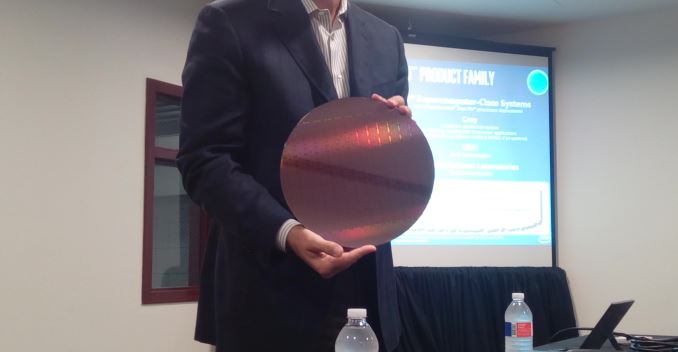
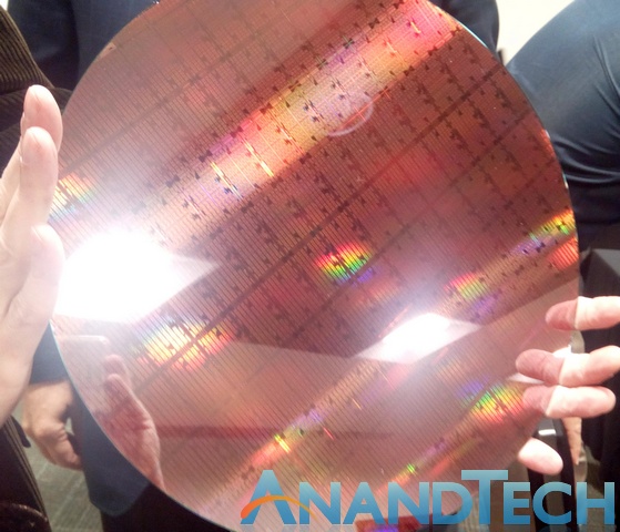
As part of a briefing at SC15, Intel had a KNL wafer on hand to show off. From this image, we can see about 9.4 dies horizontally and 14 dies vertically, suggesting a die size (give or take) of 31.9 mm x 21.4mm, or ~683 mm2. This die size comes in over what we were expecting, but comes in line with other predictions about the route of the first gen, Knights Corner, at least. Relating this to transistor counts, we have a differing story of Charlie Wuischpard (VP of Intel’s Data Center Group) stated 8 billion transistors to us at the briefing but there are reports of Diane Bryant (SVP / GM, Data Center Group) stated 7.1 billion at an Intel Nov ’14 investor briefing, but we can only find one report of the latter. This would come down to the wobbly metric of 10.4-11.7 million transistors per square millimeter.

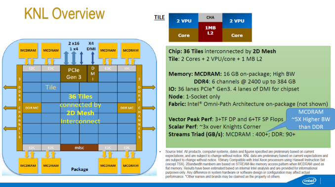
The interesting element about KNL is that where the 1st generation KNC was only available as a PCIe add-in coprocessor card, KNL can either be the main processor on a compute node, or as a co-processor in a PCIe slot. Typically Xeon Phi has an internal OS to access the hardware, but with this new model it eliminates the need for a host node – placing a KNL in a socket will give it access to both 16GB of high speed memory (the MCDRAM) as well as six memory channels for up to 384GB of DDR4, at the expense of the Intel Omni-Path controller. The KNL will also have 36 PCIe lanes which can host two more KNC co-processor cards and another four for other purposes.

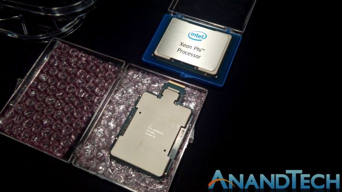
As you might expect, due to the differences we end up with the same die on different packages – one as a processor (top) and one as a co-processor which uses an internal connector for both data and Omnipath. Given the size of the die and the orientation of the cores in the slide above (we can confirm based on the die that it’s a 7×6 arrangement taking into account memory controllers and other IO), the fact that the heatspreader over the package is in a non-rectangular shape is due to the MCDRAM / custom-HMC high speed memory.

If we look into the side, the headspreader clearly does not go down onto the package all the way around, in order to deal with the on-package memory.

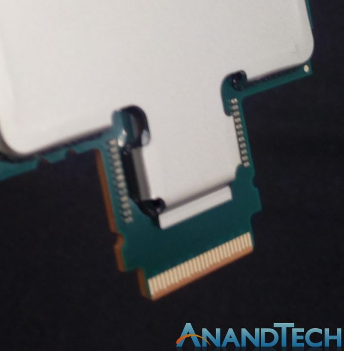
The connector end of the co-processor has an additional chip under the heatspreader, which is most likely an Intel Omni-Path connector or a fabric adaptor for adjustable designs. This will go into a PCIe card, cooler applied and then sold.

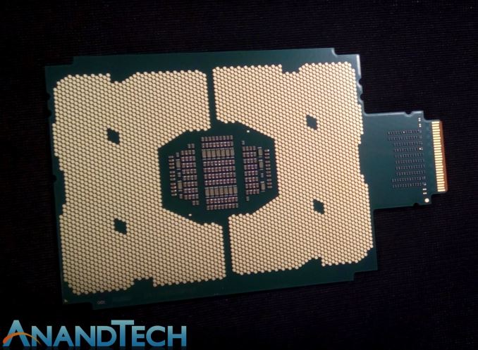
The rear of the processor is essentially the same for both.

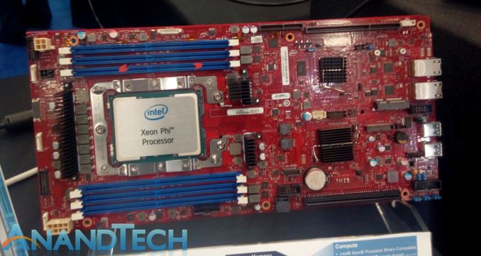
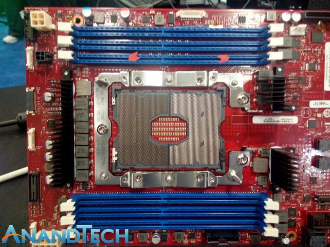
When it comes to actually putting it on a motherboard, along with the six channels of DDR4, we saw Intel’s reference board on the show floor as a representation on how to do it. A couple of companies had it on display, such as Microway, but this is a base board for others such as Supermicro or Tyan to build on or provide different functionality:

The board is longer than ATX, but thinner. I can imagine seeing one of the future variants of this in a half-width 1U blade with all six channels and two add-in boards, pretty easily. This might give six KNL in a 1U implementation, as long as you can get rid of the heat.

The socket was fairly elaborate, and it would come across that Intel has a high specification on specific pressure for heatsinks . But it is worth noting that the board design does not have an Omni-Path connection, and thus for a server rack then either additional KNLs should be added or PCIe Omni-Path cards need to be added. But this setup should help users wanting to exploit Xeon Phi in a single 1P node and MCDRAM, running the OS on the Xeon Phi itself without MPI commands to use extra nodes. There seems to be a lot of the HPC community here at SC15 who are super excited about KNL.

Regarding availability of Knights Landing, we were told that Intel has made sales for installs in Q4, but commercial availability will be in Q1. We were also told to expect parts without MCDRAM as well.

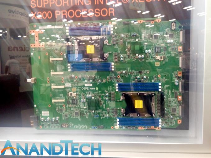
Additional: On a run through the SC15 hall, I caught this gem from SGI. It’s a dual socket motherboard, but because KNL processors have no QPI links and can only in 1P systems, this would be equivalent of two KNL nodes in one physical board.  Unfortunately they had a plastic screen in front, which distorts the images.

SuperComputing 15: Intel’s Knights Landing / Xeon Phi Silicon on Display

SuperComputing 15: Intel’s Knights Landing / Xeon Phi Silicon on Display

There are lots of stories to tell from the SuperComputing 15 conference here in Austin, but a clear overriding theme – in order to reach ‘Exascale’ (the fancy name given to where a supercomputer hits one ExaFLOP, 1018 FLOPS, in LINPACK), PCIe co-processors and accelerators are going to be a vital aspect in that. Looking at the Top500 supercomputers list that measures supercomputers in pure FLOPS, or the Green/Graph 500 lists that focus on FLOPS/watt and graph compute performance respectively (graph compute such as social networking linked lists of users (nodes) and relationships (edges)), it is clear that focused silicon is key to get peak performance and performance per watt. That focused silicon is often around NVIDIA’s Tesla high performance computing cards, FPGAs (field programmable gate arrays) from Xilinx or Altera, focused architecture designs such as PEZY, or Intel’s Xeon Phi co-processing cards.

We’ve reported on Xeon Phi before, regarding the initial launch of the first generation Knights Corner (KNC) with 6GB, 8GB or 16GB of onboard memory. These parts are listed on Intel’s ARK at $1700 to $4150 (most likely less for bulk orders) but KNC forms the backbone of the compute behind the world’s number 1 supercomputer, the Tianhe-2 in China. Over the course of SC15, more details have emerged about the 2nd generation, Knights Landing (KNL) regarding availability and memory configuration, using up to 16GB of onboard high-bandwidth memory using a custom protocol over Micron’s HMC technology and eight onboard HMC memory controllers.

As part of a briefing at SC15, Intel had a KNL wafer on hand to show off. From this image, we can see about 9.4 dies horizontally and 14 dies vertically, suggesting a die size (give or take) of 31.9 mm x 21.4mm, or ~683 mm2. This die size comes in over what we were expecting, but comes in line with other predictions about the route of the first gen, Knights Corner, at least. Relating this to transistor counts, we have a differing story of Charlie Wuischpard (VP of Intel’s Data Center Group) stated 8 billion transistors to us at the briefing but there are reports of Diane Bryant (SVP / GM, Data Center Group) stated 7.1 billion at an Intel Nov ’14 investor briefing, but we can only find one report of the latter. This would come down to the wobbly metric of 10.4-11.7 million transistors per square millimeter.

The interesting element about KNL is that where the 1st generation KNC was only available as a PCIe add-in coprocessor card, KNL can either be the main processor on a compute node, or as a co-processor in a PCIe slot. Typically Xeon Phi has an internal OS to access the hardware, but with this new model it eliminates the need for a host node – placing a KNL in a socket will give it access to both 16GB of high speed memory (the MCDRAM) as well as six memory channels for up to 384GB of DDR4, at the expense of the Intel Omni-Path controller. The KNL will also have 36 PCIe lanes which can host two more KNC co-processor cards and another four for other purposes.

As you might expect, due to the differences we end up with the same die on different packages – one as a processor (top) and one as a co-processor which uses an internal connector for both data and Omnipath. Given the size of the die and the orientation of the cores in the slide above (we can confirm based on the die that it’s a 7×6 arrangement taking into account memory controllers and other IO), the fact that the heatspreader over the package is in a non-rectangular shape is due to the MCDRAM / custom-HMC high speed memory.

If we look into the side, the headspreader clearly does not go down onto the package all the way around, in order to deal with the on-package memory.

The connector end of the co-processor has an additional chip under the heatspreader, which is most likely an Intel Omni-Path connector or a fabric adaptor for adjustable designs. This will go into a PCIe card, cooler applied and then sold.

The rear of the processor is essentially the same for both.

When it comes to actually putting it on a motherboard, along with the six channels of DDR4, we saw Intel’s reference board on the show floor as a representation on how to do it. A couple of companies had it on display, such as Microway, but this is a base board for others such as Supermicro or Tyan to build on or provide different functionality:

The board is longer than ATX, but thinner. I can imagine seeing one of the future variants of this in a half-width 1U blade with all six channels and two add-in boards, pretty easily. This might give six KNL in a 1U implementation, as long as you can get rid of the heat.

The socket was fairly elaborate, and it would come across that Intel has a high specification on specific pressure for heatsinks . But it is worth noting that the board design does not have an Omni-Path connection, and thus for a server rack then either additional KNLs should be added or PCIe Omni-Path cards need to be added. But this setup should help users wanting to exploit Xeon Phi in a single 1P node and MCDRAM, running the OS on the Xeon Phi itself without MPI commands to use extra nodes. There seems to be a lot of the HPC community here at SC15 who are super excited about KNL.

Regarding availability of Knights Landing, we were told that Intel has made sales for installs in Q4, but commercial availability will be in Q1. We were also told to expect parts without MCDRAM as well.

Additional: On a run through the SC15 hall, I caught this gem from SGI. It’s a dual socket motherboard, but because KNL processors have no QPI links and can only in 1P systems, this would be equivalent of two KNL nodes in one physical board.  Unfortunately they had a plastic screen in front, which distorts the images.

The AMD A8-7670K APU Review: Aiming for Rocket League

Over the past couple of years, AMD has slowly released their mainstream brand of Kaveri processors. In turn, we have reviewed them, and they consistently aim to provide a midrange integrated gaming option, especially for those on a budget. The recent release of the A8-7670K was perhaps not that exciting, as AMD is filling up their product stack with new parts, taking advantage of an improved manufacturing process and aggressive binning. To that end, we’re taking a different tack with this review. Alongside the regular tests, we also corralled Rocket League (an amazingly simple yet popular take on car football/soccer that sits on the precipice of e-sports glory) into a benchmark aimed at those sub-$600 gaming systems.