CPUs


Intel Announces Cyclone 10 FPGAs for IoT Devices

Intel Announces Cyclone 10 FPGAs for IoT Devices

Intel this week has announced its new portfolio of FPGAs designed for small form-factor and/or low-power Internet-of-Things devices, specifically in the fields of automotive, industrial, audio/visual and vision applications. The Cyclone 10 GX and Cyclone 10 LP FPGAs formally belong to a single family of products, but both have different capabilities and were developed for different needs.

The Intel Cyclone 10 GX FPGAs are designed for applications that need relatively high performance (up to 134 GFLOPS, IEEE 754 single-precision) and advanced I/O capabilities. The new FPGAs contain up to 220,000 logic elements, up to 80,330 adaptive logic modules (ALMs) with 8-input look-up tables (LUT), support 10 G transceivers as well as a PCIe 2.0 x4 IP block to connect to CPUs and other devices. Among devices that will use the Cyclone 10 GX FPGAs Intel names industrial machine vision, smart city surveillance, video streaming, robotics, machine tools and other devices. The 10 GX family is made on TSMC’s 20nmSoC planar process, in line with what we perhaps expect as Intel is working through Altera roadmaps set before the acquisition.

By contrast, the Intel Cyclone 10 LP FPGAs are aimed at low-power/low-cost applications, such as sensor fusion, motor controls, interfacing, I/O expansion for CPUs and so on. For example, if an application needs to combine data from multiple sensors, the Cyclone 10 LP will do the job, but the actual processing will be performed by something more powerful. The FPGAs contain 6,000 – 120,000 logic elements, DSP blocks (up to 288 18×18 multipliers), integrated PLLs, 65 – 230 LVDS channels and so on.  

Both families of the Cyclone 10 FPGAs are compliant with the IEC 61508 machinery directive safety standard (in fact, Intel says that it is the first FPGA vendor to obtain the appropriate device and tool qualification), which in case of a chip probably indicates its reliability during continuous operation. 

Intel Cyclone 10 FPGAs
  Cyclone 10 GX Cyclone 10 LP
Logic elements (LEs) 85,000 – 220,000 6,000 – 120,000
Adaptive logic modules (ALMs) 31,000 – 80,330
ALM registers 124,000 – 321,320
Variable-precision DSP blocks 84 – 192
18 x 19 multipliers 168 – 384
18 x 18 multipliers 15 – 288
Peak fixed-point peformance (GMACS) 151 – 346
Peak floating-point performance (GFLOPS) 59 – 134
Voltage Core voltage: 0.9 V
I/O Voltage: Various
1.0 and 1.2 V
Process Technology 20 nm (TSMC CLN20SOC) unknown
I/O
Global clock networks 32 10 – 20
Maximum user I/O pins 192 – 284 176 – 525
Maximum LVDS pairs 1.4 Gbps (RX or TX) 72 – 118  
Maximum LVDS channels 65 – 230
Maximum transceiver count (10.3 Gbps) 4 – 12
Maximum 3V I/O pins 48
PCIe 2.0 x4 hard IP blocks 1
Memory devices supported DDR3, DDR3L, LPDDR3
Packaging
E144 pin 22 x 22 mm, 0.5 mm pitch
M164 pin 8 x 8 mm, 0.5 mm pitch
U256 pin 14 x 14 mm, 0.8 mm pitch
U484 pin 19 x 19 mm, 0.8 mm pitch
F484 pin 23 x 23 mm, 1.0 mm pitch
F672 pin 27 x 27 mm, 1.0 mm pitch
F780 pin 29 x 29 mm, 1.0 mm pitch

Intel’s Cyclone 10-series FPGAs, as well as evaluation kits and boards on their base, will be available in the second half of 2017. In addition to hardware, Intel also plans to release its Quartus programming software that supports the new FPGAs.

Related Reading:

Intel Announces Cyclone 10 FPGAs for IoT Devices

Intel Announces Cyclone 10 FPGAs for IoT Devices

Intel this week has announced its new portfolio of FPGAs designed for small form-factor and/or low-power Internet-of-Things devices, specifically in the fields of automotive, industrial, audio/visual and vision applications. The Cyclone 10 GX and Cyclone 10 LP FPGAs formally belong to a single family of products, but both have different capabilities and were developed for different needs.

The Intel Cyclone 10 GX FPGAs are designed for applications that need relatively high performance (up to 134 GFLOPS, IEEE 754 single-precision) and advanced I/O capabilities. The new FPGAs contain up to 220,000 logic elements, up to 80,330 adaptive logic modules (ALMs) with 8-input look-up tables (LUT), support 10 G transceivers as well as a PCIe 2.0 x4 IP block to connect to CPUs and other devices. Among devices that will use the Cyclone 10 GX FPGAs Intel names industrial machine vision, smart city surveillance, video streaming, robotics, machine tools and other devices. The 10 GX family is made on TSMC’s 20nmSoC planar process, in line with what we perhaps expect as Intel is working through Altera roadmaps set before the acquisition.

By contrast, the Intel Cyclone 10 LP FPGAs are aimed at low-power/low-cost applications, such as sensor fusion, motor controls, interfacing, I/O expansion for CPUs and so on. For example, if an application needs to combine data from multiple sensors, the Cyclone 10 LP will do the job, but the actual processing will be performed by something more powerful. The FPGAs contain 6,000 – 120,000 logic elements, DSP blocks (up to 288 18×18 multipliers), integrated PLLs, 65 – 230 LVDS channels and so on.  

Both families of the Cyclone 10 FPGAs are compliant with the IEC 61508 machinery directive safety standard (in fact, Intel says that it is the first FPGA vendor to obtain the appropriate device and tool qualification), which in case of a chip probably indicates its reliability during continuous operation. 

Intel Cyclone 10 FPGAs
  Cyclone 10 GX Cyclone 10 LP
Logic elements (LEs) 85,000 – 220,000 6,000 – 120,000
Adaptive logic modules (ALMs) 31,000 – 80,330
ALM registers 124,000 – 321,320
Variable-precision DSP blocks 84 – 192
18 x 19 multipliers 168 – 384
18 x 18 multipliers 15 – 288
Peak fixed-point peformance (GMACS) 151 – 346
Peak floating-point performance (GFLOPS) 59 – 134
Voltage Core voltage: 0.9 V
I/O Voltage: Various
1.0 and 1.2 V
Process Technology 20 nm (TSMC CLN20SOC) unknown
I/O
Global clock networks 32 10 – 20
Maximum user I/O pins 192 – 284 176 – 525
Maximum LVDS pairs 1.4 Gbps (RX or TX) 72 – 118  
Maximum LVDS channels 65 – 230
Maximum transceiver count (10.3 Gbps) 4 – 12
Maximum 3V I/O pins 48
PCIe 2.0 x4 hard IP blocks 1
Memory devices supported DDR3, DDR3L, LPDDR3
Packaging
E144 pin 22 x 22 mm, 0.5 mm pitch
M164 pin 8 x 8 mm, 0.5 mm pitch
U256 pin 14 x 14 mm, 0.8 mm pitch
U484 pin 19 x 19 mm, 0.8 mm pitch
F484 pin 23 x 23 mm, 1.0 mm pitch
F672 pin 27 x 27 mm, 1.0 mm pitch
F780 pin 29 x 29 mm, 1.0 mm pitch

Intel’s Cyclone 10-series FPGAs, as well as evaluation kits and boards on their base, will be available in the second half of 2017. In addition to hardware, Intel also plans to release its Quartus programming software that supports the new FPGAs.

Related Reading:
Intel Announces the Xeon E7-8894 v4 CPU: 24 Cores at 2.4 GHz for $8898

Intel Announces the Xeon E7-8894 v4 CPU: 24 Cores at 2.4 GHz for $8898

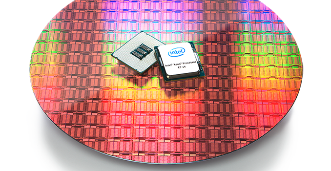
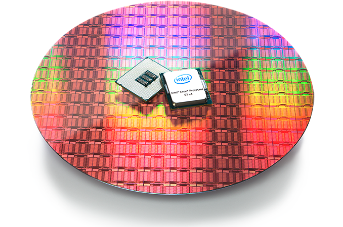
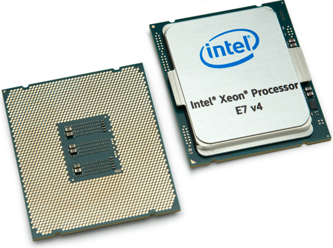
In the past week, Intel has launched a new halo CPU – its highest-performing multi-core CPU for multi-socket mission-critical servers, the Xeon E7-8894 v4. The new processor is based on the Broadwell-EX die and has approximately a 200 MHz higher base frequency than its direct predecessor, released in Q2 2016. Intel said that the new CPU has set a number of records in various benchmarks. Intel’s customers interested in the chip will also have to pay a record price too.

The flagship Intel Xeon E7-8894 v4 processor features the Broadwell-EX XCC (extreme core-count) die and has 24 cores with Hyper-Threading technology, 60 MB of L3 cache, 165 W TDP, a default frequency of 2.4 GHz and a turbo frequency of up to 3.4 GHz. Like other Broadwell-EX XCC CPUs, the new chip has quad-channel DDR3/DDR4 memory controller support and can manage up to ~3 TB of DRAM per socket (when used in conjunction with four Jordan Creek 2 scalable memory buffers). The CPUs are also equipped with 32 PCIe 3.0 lanes and three 9.6 GT/s QPI links for multi-socket environments.

Intel E7-8800 v4 Xeon Family
  E7-8867 v4 E7-8870 v4 E7-8880 v4 E7-8890 v4 E7-8894
v4
  E7-8891 v4 E7-8893 v4
TDP 165 W 140 W 150 W 165 W 165 W 140 W
Cores 18 / 36 20 / 40 22 / 44 24 / 48 10 / 20 4 / 8
Base Freq 2400 2100 2200 2200 2400 2800 3200
Turbo 3300 3000 3300 3400 3500 3500
L3 Cache 45 MB 50 MB 55 MB 60 MB 60 MB 60 MB
QPI (GT/s) 3 × 9.6 3 x 9.6 3 x 9.6
DRAM DDR4-1866
DDR3-1600
DDR4-1866
DDR3-1600
PCIe PCIe 3.0 x32 3.0 x32 3.0 x32
Price $4672 $4762 $5895 $7174 $8898 $6841 $6841

Intel’s multi-core Xeon E7 processors are designed for various heavy-duty servers with four, eight or more sockets (to support more than eight sockets special third-party node controllers are required). Such mission-critical machines typically to be available 24/7/365 and this is why the Xeon E7 v4 and the Broadwell-EX range has a host of various RAS (reliability, availability, serviceability) features. The Xeon E7-8894 v4 CPU has exactly the same set of capabilities as its direct predecessor, the Xeon E7-8890 v4 released last year.

Intel claims that due to increased default frequency (and obviously because of the core count in general), the Xeon E7-8894 v4 sets a number of performance records in various general, server, HPC, big data analytics, business processing, database and other benchmarks, such as SPECint_base2006, SPECompG_2012, and so on.

The Intel Xeon E7-8894 v4 processor carries a tray price of $8898, which is the highest price of an Intel mass-produced CPU ever. Its predecessor on the top spot in the range, the 24-core Xeon E7-8890 v4 (which runs at 2.2 GHz) is priced at $7174 and still sits at its original tray price. As always, there are customers willing to pay such sums of money for server CPUs that deliver certain levels of performance. Moreover, there are workloads that benefit from a +200MHz (9%) performance increase so significantly (from a financial point of view to the owners of the machines) that it justifies paying extra 24% (or $1724) for a 200 MHz frequency increase (provided that this is the only advantage that this CPU has over the E7-8890 v4).

Intel Xeon E-Series Families (February 2017)*
  E3-1200 v5 E3-1500 v5 E5-1600 v4
E5-2600 v4
E5-4600 v4
E7-4800 v4 E7-8800 v4
Core Family Skylake Skylake Broadwell Broadwell Broadwell
Core Count 2 to 4 2 to 4 4 to 22 8 to 16 4 to 24
Integrated Graphics Few, HD 520 Yes, Iris Pro No No No
DRAM Channels 2 2 4 4 4
Max DRAM Support (per CPU) 64 GB 64 GB 1536 GB 3072 GB 3072GB
DMI/QPI DMI 3.0 DMI 3.0 2600: 1xQPI
4600: 1xQPI
3 QPI 3 QPI
Multi-Socket Support No No 2600: 1S/2S
4600: 1S/2S
1S, 2S or 4S Up to 8S
PCIe Lanes 16 16 40 32 32
Cost $213 to
$612
$396 to
$1207
$294 to
$7007
$1223 to
$3003
$4061 to
$8898
Suited For Entry Workstations QuickSync,
Memory Compute
High-End Workstation Many-Core Server World Domination

*Intel also has the E3-1500M v5 and E3-1500M v6 mobile parts which are left out of this table

We’ve asked Intel to disclose the official per-core turbo numbers for comparison to their other chips, as well as a full range of DRAM support depending on memory type and memory density. We will update this news piece as we get more information.

Related Reading:

Intel Confirms 8th Gen Core on 14nm, Data Center First to New Nodes

Intel Confirms 8th Gen Core on 14nm, Data Center First to New Nodes

A quick news piece on information coming out of Intel’s annual Investor Day in California. As confirmed to Ashraf Eassa by Intel at the event, Intel’s 8th Generation Core microarchitecture will remain on the 14nm node. This is an interesting development with the recent launch of Intel’s 7th Generation Core products being touted as the ‘optimization’ behind the new ‘Process-Architecture-Optimization’ three-stage cadence that had replaced the old ‘tick-tock’ cadence. With Intel stringing out 14nm (or at least, an improved variant of 14nm as we’ve seen on 7th Gen) for another generation, it makes us wonder where exactly Intel can promise future performance or efficiency gains on the design unless they start implementing microarchitecture changes.

Despite this, if you were to believe supposed ‘leaked’ roadmaps (which we haven’t confirmed from a second source as of yet), the 8th Generation product ‘Cannon Lake’ is more geared towards the Y and U part of Intel’s roadmap. This would ring true with a mobile first strategy that Intel has mirrored with recent generations such that the smaller, low power chips are off the production line for a new product first, however we’d also expect 10nm to also be in the smaller chips first too (as demonstrated at CES). Where Cannon Lake will end up in the desktop or enterprise segment however remains to be seen. To put something a bit more solid into this, Ashraf also mentioned words from Dr. Venkata ‘Murthy’ Renduchintala, VP and GM of Client and IoT:

‘Murthy referred to it at the event, process tech use will be ‘fluid’ based on segment’.

If one read too much into this, we may start seeing a blend of process nodes for different segments at the same time for different areas of the market. We already do have that to some extent with the mainstream CPUs and the HEDT/Xeon families, but this phrasing seems that we might get another split between consumer products or consumer and enterprise. We may get to a point where Intel’s ‘Gen’ naming scheme for its CPUs covers two or more process node variants.

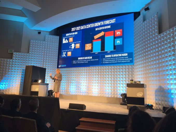
Speaking of the Enterprise segment, another bit of information has also surfaced, coming from a slide during a talk by Diane Bryant (EVP/GM of Data Center) and posted online by Ashraf. The slide contains the words ‘Data center first for next process node’

We can either talk about process node in terms of the ‘number’, either 14nm/10nm/7nm, or by variants within that process (high power, high efficiency). One might suspect that this means Intel is moving hard and fast with 10nm for Xeons and big computing projects, despite showing off 10nm silicon at CES earlier this year. That being said, it’s important to remember that the data center market is large, and includes high-density systems with many cores, such as Atom cores, and Intel did recently open up its 10nm foundry business to ARM Artisan IP projects. So while the slide does say ‘Data center first’, it might be referring to DC projects based on ARM IP in that segment rather than big 4-24+ core Xeons. At this stage of the game it is hard to tell.

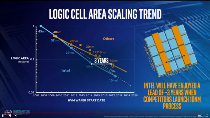
On top of all this, Intel still has extreme confidence in its foundry business. An image posted by Dick James of Siliconics from the livestream shows Intel expects to have a three-year process node advantage when its competitors (Samsung, TSMC) start launching 10nm:

I’ve been brief with this news for a reason – at this point there are a lot of balls in the air with many different ways to take this information, and the Investor Day is winding down on talks and finishing with smaller 1-on-1 meetings. We may get further clarification on this news as the day goes on.

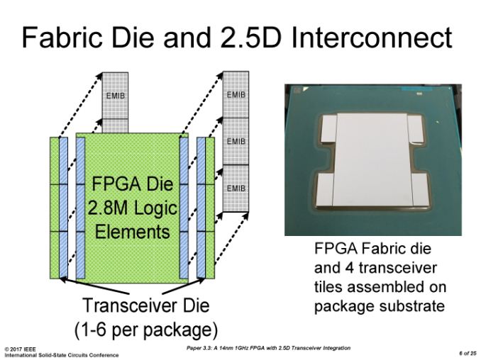
Update 1: On speaking with Diane Bryant, the ‘data center gets new nodes first’ is going to be achieved by using multiple small dies on a single package. But rather than use a multi-chip package as in previous multi-core products, Intel will be using EMIB as demonstrated at ISSCC: an MCP/2.5D interposer-like design with an Embedded Multi-Die Interconnect Bridge (EMIB).


An Intel Slide from ISSCC, via PC Watch

Initially EMIB was thought of as a technology relating to Intel’s acquisition of Altera and potential future embedded FPGA designs, and given the slide above and comments made at the Investor Day, it seems there are other plans for this technology too. The benefit of using multiple smaller dies over a large monolithic 600mm2 die is typically related to cost and yield, however the EMIB technology also has to be up to par and there may be a latency or compatibility trade-off.