
As part of today’s announcements, we’re able to provide more information on ARM’s new “Built on ARM Cortex Technology” license. The license was first officially revealed in ARM’s quartely financial call back in February, however at the time the company wasn’t ready to talk about the exact details of this new license.
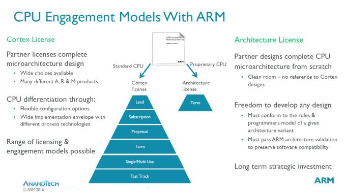
We covered ARM’s business and licensing models back a few years ago in a dedicated article which goes into more depth what kind of options vendors have when deciding to license an ARM IP. ARM likes to represent the licensing model in a pyramid shape with increasing cost and involvement the higher you get on the pyramid. Until now vendors had two main choices: Use one of the various available Cortex licenses, or get an architectural license and develop one’s own microarchitecture based on ARM’s ISA.
The former licensing options varied depending on what kind of engagement and deployment a vendor is looking for. Lead licensees for example get early access to new microarchitectures but also have to pay more for this access and it’s possible that they will have to deal with still immature toolkits and documentation, both which would then require more invovement and investment on their part. Vendors who are willing to wait a bit more or who aren’t looking in an as deep engagement are able to use some of the cheaper licenses and more mature tools and documentation.
The common limitation of all current Cortex licenses however is that a vendor is not able to change any aspect of the microarchitecture. If a customer needed a feature that ARM’s cores didn’t provide, they had to go with an architectural license and develop their own microarchitecture from scratch. Currently examples of such licensees with shipping custom microarchitectures include Apple, Qualcomm and Samsung.
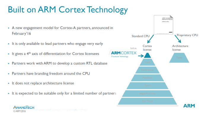
The new license being detailed today is the “Built on ARM Cortex Technology” license, which is quite a mouthfull and will unofficially refer to as “Built on Cortex”/BoC from here on. The new BoC license represents a new “tip of the pyramid” for Cortex licenses with even greater engagement than that of lead licensees.
The new license allows vendors to request changes of an ARM microarchitecture and use this customized IP in their products. The way this works is that basically ARM provides its engineering and design services to the vendor who wants a certain aspect of an “off-the-shelf” Cortex design customized. Under the license’s terms, ARM still owns and controls the IP, however the changes requested for that particular vendor’s design is not shared or made available to other vendors.


An example of a customization that a vendor would be able to request is the instruction window size. An increase in the instruction window size would increase the IPC of a microarchitecture, however this can cause higher area and power which would need to be compensated by more implementation work by the vendor.
While ARM didn’t want to go into details of what other customization options a vendor would have, they say that it will have a rather limited scope and things such as altering decoder width or changing the execution resources of a microarchitecture are beyond the scope of the license. In general, it seems more that the license is meant to allow vendors to tweak and configure the knobs on some aspects of a microarchitecture rather than do significant changes to the way the µarch works.
What is in my view the most important and controversial aspect of the new license is that it allows vendors full branding freedom on this customized CPU design. This means that a Built on Cortex licensee is free to give the resulting new core any name it sees fit. We’ll however still be able to differentiate the core from a full custom microarchitecture as ARM still requires a disclaimer / footnote / subtitle with the “Built on ARM Cortex Technology” phrase.
In February ARM disclosed that Qualcomm is the first costumer signed up for this license, and what this means for the Snapdragon SoC lineup is currently still unclear. If this new licensing model will be able to allow vendors to truly differentiate their products beyond just the marketing aspect is something we won’t know until the first designs come out and will be tested, and until then, the verdict on ARM’s new license is still open.