The month the Bluetooth SIG has taken the wraps off of their latest standards project: an addition to the Bluetooth specification that enables creation of large networks of devices. Dubbed “Bluetooth Mesh”, the new standard is designed for smart homes, public and manufacturing facilities. An extension of the Bluetooth LE protocol, the Bluetooth SIG hopes that the first products supporting the Bluetooth Mesh specification will be quickly available in the coming months as the new technology does not require principally new hardware.
Bluetooth Evolution
The Bluetooth technology was originally developed in the late 1990s to enable wireless device-to-device communications. This device-to-device tech has been evolving since 1997 by improving transfer rates, extending range, and improving reliability. In the early 2000s, researchers and product developers determined that there were many devices that could benefit from short-burst wireless connectivity, but did not need a fully-fledged Bluetooth implementation due to power consumption and size concerns. To this end, developers from Nokia and other companies started to design a low-power version of Bluetooth that was first marketed under the Wibree trademark in 2006 and then became a part of the Bluetooth 4.0 spec under the Bluetooth Smart (Bluetooth LE) trademark.
Bluetooth LE introduced a one-to-many communication paradigm to the standard, enabling various new usage models and applications, such as item finding beacons or way finding beacons. Meanwhile, device-to-device and device-to-many-devices Bluetooth interconnections ultimately use a star topology, and thus such networks have limits to their range and the number of devices in a network, which can inhibit their usage models.

With the introduction of the Bluetooth Mesh standard, the Bluetooth SIG is bringing a many-to-many communication paradigm to the standard. As the name implies, Bluetooth Mesh enables building large-scale device networks with a mesh topology and thus extends the range of a single Bluetooth network virtually to infinity (mind latency and other factors though). In turn, such large networks open up new usage models for the technology, particularly in the field of IoT devices.
How It Works
At a high level, Bluetooth Mesh uses the Bluetooth 4.0 LE protocol to transport data between devices (nodes). This means that from a data transmission point of view, nearly everything has already been specified, from low layer radios to encryption to application layers.
What Bluetooth Mesh adds on top of Bluetooth LE is an ability to retransmit data (a message) from one device to other devices that are in direct radio range (a single hop away) until it reaches the destination — the address it is sent to — using the so-called managed flooding technique. Managed flooding allows the receiver to determine how many hops it’s away from the sender, and thus disable message relaying further than it is needed (i.e., set the maximum number of hops over which the message is retransmitted), thus preserving power and saving the bandwidth of the whole network. This technique ensures that the message always reaches its destination potentially using various paths even if certain nodes fail. Moreover, by not using routing devices, Bluetooth Mesh networks become cheaper and more reliable — messages always get to their destinations no matter what happens to individual nodes within a network (so long as there’s a path).

Under the hood, Bluetooth Mesh networks consist of relay nodes that can retransmit messages, and low-power nodes that connect to relay nodes to periodically transmit or receive data using a mechanism called friendship (i.e., each LP node has a Friend). Low-power nodes could be various sensors or beacons that only use short-burst data transmissions with their “Friends”, which then retransmit their data to other nodes.
The Bluetooth SIG says that a single Bluetooth Mesh network can contain up to 32,767 elements (a node has at least one element, or addressable entity), but admits that in the real world such networks will typically consist of at most thousands, rather than tens of thousands of devices.
When it comes to bandwidth, the gross air data rate of the Bluetooth LE is 1 Mb/s (at maximum transmit power of 10 mW), but this figure does not account for protocol overhead. There are reports that the maximum achievable BLE data rate is around 10 KB/s depending on the devices used. Such data rates are not a problem for point-to-point communications within the contemporary star network topology. However what happens when hundreds of devices start passing numerous messages over the mesh network remains to be seen. Bandwidth, latency (6 ms per hop – the standard for the Bluetooth LE) and lack of priority attributes for data packets could be limiting factors for Bluetooth Mesh adoption in environments that generate loads of data.
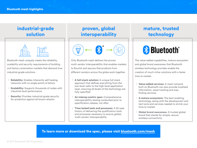
It is important to note that the Bluetooth SIG made interoperability a part of the specification development process, and therefore thousands of interoperability tests have already been conducted. This is not exactly surprising as the Bluetooth Mesh spec builds up Bluetooth LE, and therefore existing Bluetooth 4/5-capable chips can support the new technology. Meanwhile, actual contemporary devices may or may not receive firmware and software upgrades to enable Bluetooth Mesh support. Some device makers interested in addressing smart home and other applications are more likely to enable the new spec on existing products, but others are more likely to qualify future products for the new tech.
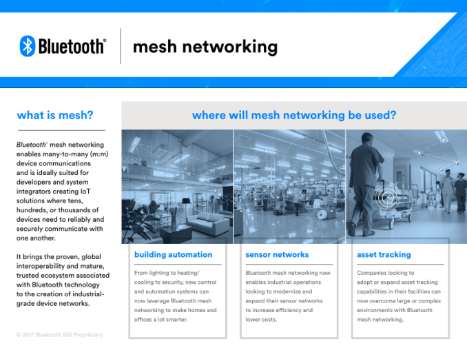
Use Cases and Competition
At present, the Bluetooth SIG and its members are pursuing several key applications for Bluetooth Mesh: smart home, lighting, beaconing, automation, and asset tracking applications. For example, integrating relay-capable nodes into lighting devices across a home extends range of the network to the whole building. Each of the multiple relay nodes installed in every room can then connect to various low-power nodes, such as temperature sensors, thermostats, window blind controls, and so on. In a warehouse, a robot could navigate its way across the building without any network range-related constraints while enabling operators to track its whereabouts.
The Bluetooth SIG is certainly not alone with its mesh-networking standard for IoT applications, both in general and smart homes in particular. There is ZigBee that is used for various smart home appliances already, there are proprietary technologies, and Wi-Fi HaLow is incoming. A natural advantage that the Bluetooth SIG and its members have is that there are hundreds of millions of Bluetooth-enabled devices produced and sold every year, and therefore the majority of upcoming smartphones, smart TVs, notebooks, tablets, and other products will have the ability to be compatible with the Bluetooth Mesh specification. As a result, it will make a lot of sense for developers of smart home appliances to design devices compatible with Bluetooth Mesh — millions of consumers will have compatible devices in about a year from now, and this is a huge number for an emerging market. Meanwhile, when it comes to custom automation or industrial applications, it remains to be seen which technology developers prefer for their large-scale device networks.
Preliminary Thoughts
Nowadays there are billions of Bluetooth LE-enabled devices, and in the coming years their number will grow further not only because people will buy more smartphones, but because a lot of brand new device types will emerge. The Bluetooth Mesh specification enables building large-scale device networks without the need to launch any new hardware, and thus makers of smart home appliances (and other devices) may begin quickly adopting the new tech in the coming months.
Relying on the Bluetooth LE specification and the managed flooding message transport technique ensures that Bluetooth Mesh-based large-scaled device networks will have predictable performance (RF interference withstanding), known security mechanisms, high reliability, and relatively low costs. Moreover, to a degree the usage Bluetooth LE eliminates the chicken and egg dilemma for the new standard early in its life, as supporting devices are already here. However, it is not completely clear how the number of nodes per single network affects its performance, and that will be a very important factor once large networks consisting of hundreds or thousands of nodes are built.
Keeping in mind that Bluetooth connectivity is ubiquitous nowadays, Bluetooth Mesh has a good chance to become a very popular wireless standard for smart homes and other applications, provided that it can deliver the right performance and ensure compatibility and interoperability between devices from different vendors. The Bluetooth SIG says that interoperability is nearly guaranteed for Bluetooth Mesh supporting devices, but we will have to see how that pans out ourselves.
Otherwise, while developers of smart devices can start building Bluetooth Mesh products based on silicon solutions designed by others, they will still have to complete the long-standing Bluetooth qualification and/or declaration processes in order to ensure that their products satisfy the Bluetooth license the requirements and to pay the appropriate fees. This is not going to be a problem for the established players, but may pose a small challenge for small startups.
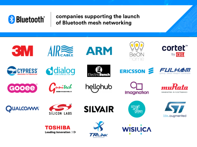
Finally, the Bluetooth SIG is naming a number of semiconductor manufacturers, software developers, and device manufacturers as among Bluetooth Mesh’s early adopters. This include 3M, ARM, Ericsson, STMicroelectronics, Qualcomm, Toshiba, and others. While the organization does not announce any final products, it makes it clear that Bluetooth Mesh is has manufacturer support at both the silicon and on-device levels. Moreover, there are turnkey silicon and software solutions available from companies like Cypress, Silicon Labs, and Wisilica to build devices compatible with Bluetooth Mesh. Ultimately, the sky looks blue for the Bluetooth Mesh to take off, but its actual market acceptance will depend on the adoption of IoT devices for homes, offices, and production facilities.