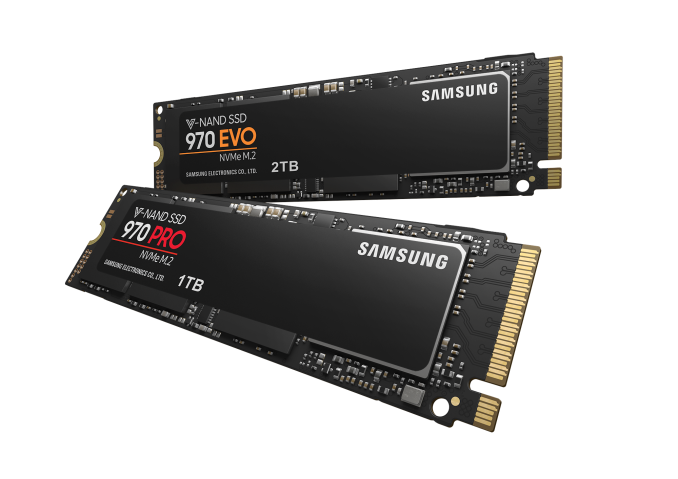
Samsung has announced the third generation of their high-end consumer NVMe SSDs. The new 970 PRO and 970 EVO M.2 NVMe SSDs use a newer controller and Samsung’s latest 64-layer 3D NAND flash memory. The outgoing 960 PRO and 960 EVO were first announced in September 2016 and shipped that fall, so they have had a fairly long run as Samsung’s flagship consumer SSDs.
There are no big surprises from today’s announcement. Samsung’s transition to 64-layer 3D NAND has been underway for a year, and the retail SATA lineup migrated to the fourth-generation 3D NAND earlier this year. This generation of NAND includes a 512Gb TLC die that allows for 1TB in a single BGA package, so squeezing 2TB onto a single-sided M.2 2280 card is no longer a challenge.
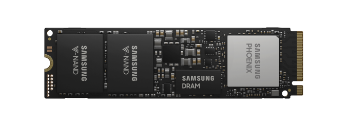
The Samsung Phoenix controller used in the 970s has been on our radar for a long time after appearing on many of Samsung’s recent NVMe SSDs for other markets: the PM981 client SSD for OEMs, the PM983 enterprise SSD that is being used to promote Samsung’s new NF1 (formerly NGSFF) form factor, and the high-end enterprise Z-SSD SZ985.
Read Our Samsung PM981 SSD Review
Samsung’s retail NVMe SSD product numbering is now out of sync with their OEM and enterprise SSDs. This is because the Samsung PM971 wasn’t a direct replacement for anything in the 96x generation. Instead, the PM971 is a low-end BGA SSD featuring Samsung’s Photon controller instead of the 96x generation’s Polaris or the current Phoenix. BGA SSDs are obviously not a good fit for the retail SSD market, and even when mounted on M.2 cards the PM971 would have had a fairly small audience. Samsung’s retail NVMe SSDs aren’t skipping over the 970 generation, but their other high-end NVMe drives did.
Samsung is still using MLC NAND for the PRO series and TLC NAND for the EVO series. However, it is clear that the TLC-based EVO is the more important product for Samsung. The PRO series has been reduced back down to just two capacities (512GB and 1TB), while the EVO now spans from 250GB up to 2TB. The EVO series now also matches the PRO’s 5-year warranty term. Other manufacturers have started to abandon MLC NAND completely for their consumer product lines. Samsung isn’t quite there yet, but the PRO is looking like even more of a niche product this time around. We have not seen a MLC-based SM981 drive, so it seems likely that the client OEM product line is done using MLC NAND.
| Samsung 970 EVO Specifications |
| Capacity |
250 GB |
500 GB |
1 TB |
2 TB |
| Interface |
PCIe 3 x4 NVMe 1.3 |
| Form Factor |
M.2 2280 Single-sided |
| Controller |
Samsung Phoenix |
| NAND |
Samsung 64-layer 256Gb 3D TLC |
Samsung 64L 512Gb 3D TLC |
| LPDDR4 DRAM |
512 MB |
1 GB |
2 GB |
| SLC Write Cache |
Dedicated |
4 GB |
4 GB |
6GB |
6 GB |
| Dynamic |
9 GB |
18 GB |
36 GB |
72 GB |
| Sequential Read |
3400 MB/s |
3500 MB/s |
| Sequential Write (SLC Cache) |
1500 MB/s |
2300 MB/s |
2500 MB/s |
2500 MB/s |
| Sequential Write (TLC) |
300 MB/s |
600 MB/s |
1200 MB/s |
1250 MB/s |
| 4KB Random Read |
QD1 |
15k IOPS |
| QD128 |
200k IOPS |
370k IOPS |
500k IOPS |
500k IOPS |
| 4KB Random Write |
QD1 |
50k IOPS |
| QD128 |
350k IOPS |
450k IOPS |
450k IOPS |
480k IOPS |
| Active Power |
Read |
5.4 W |
5.7 W |
6 W |
6 W |
| Write |
4.2 W |
5.8 W |
6 W |
6 W |
| Idle Power |
APST On |
30 mW |
| PCIe L1.2 |
5 mW |
| Write Endurance |
150 TB |
300 TB |
600 TB |
1200 TB |
| Warranty |
5 years |
| MSRP |
$119.99 (48¢/GB) |
$229.99 (46¢/GB) |
$449.99 (45¢/GB) |
$849.99 (42¢/GB) |
We were impressed with the PM981 drives we had the opportunity to test in November. We found that the combination of updated NAND and the new Phoenix controller provided a solid generational boost over the 960 EVO, often bringing performance up to the level of the 960 PRO and occasionally surpassing it. The retail 970s are a bit overdue, because several recent competing NVMe SSDs had made it clear that the 960s were losing the lead. The 970 EVO on its own probably won’t be enough for Samsung to reestablish an undisputed lead in M.2 SSD performance.
Compared to its predecessor, the 970 EVO promises a small improvement in sequential read speed, and a more substantial boost to sequential write speed for all but the smallest 250GB model. Peak random access performance is also substantially improved, but again the 250GB model gets left out, and is actually rated as slower than the 960 EVO 250GB.
The warranty on the EVO has been extended from three years to five years, and the write endurance ratings have been increased by 50% to retain almost the same drive writes per day rating.
The 970 EVO will debut with prices slightly lower than the launch MSRPs for the 960 EVO. In between the two product launches, a severe industry-wide shortage of flash memory kept prices high, but now that most NAND flash manufacturers have their 64L 3D NAND production in full swing, retail prices are improving.
Samsung has dropped the 2TB option from the PRO lineup, replacing it with a 2TB 970 EVO that is about a third cheaper and will likely be much more popular. That 2TB 970 EVO is the only model using Samsung’s 512Gb 64L 3D TLC die, while the smaller models use the 256Gb version.

| Samsung 970 PRO Specifications |
| Capacity |
512 GB |
1 TB |
| Interface |
PCIe 3 x4 NVMe 1.3 |
| Form Factor |
M.2 2280 Single-sided |
| Controller |
Samsung Phoenix |
| NAND |
Samsung 64-layer 3D MLC V-NAND |
| LPDDR4 DRAM |
512 MB |
1 GB |
| Sequential Read |
3500 MB/s |
| Sequential Write |
2300 MB/s |
2700 MB/s |
| 4KB Random Read |
QD1 |
15k IOPS |
| QD128 |
370k IOPS |
500k IOPS |
| 4KB Random Write |
QD1 |
55k IOPS |
| QD128 |
500k IOPS |
| Active Power |
Read |
5.2 W |
| Write |
5.2 W |
5.7 W |
| Idle Power |
APST On |
30 mW |
| PCIe L1.2 |
5 mW |
| Write Endurance |
600 TB |
1200 TB |
| Warranty |
5 years |
| MSRP |
$329.99 (64¢/GB) |
$629.99 (62¢/GB) |
The 970 PRO’s performance specs aren’t too different from the 970 EVO. Many of the ratings are the same, and the ones that differ are mostly better by just 3-11% for the PRO. There are just two major exceptions to this. First, the PRO doesn’t rely on SLC write caching so it can maintain its write speed far longer than the EVO. Second, the rated write endurance of the 970 PRO is twice that of the EVO, going from just over 0.3 Drive Writes Per Day to 0.6 DWPD. Neither of these are an important factor for ordinary consumer use cases, but they help the 970 PRO retain some shine as a premium product.
The 970 PRO’s improvements over the 960 PRO are mostly for random I/O performance, where both drives are now rated to hit 500k IOPS for random writes, given sufficient queue depth. As with the EVO, rated write endurance has been increased by 50%, but the PRO’s warranty remains at 5 years. The MSRPs for the 970 PRO are the same as the the launch prices for the 960 PRO.
The 970 PRO and 970 EVO will be available for purchase worldwide beginning May 7, 2018.
Related Reading


