ARM Announces Mali-G72: Bifrost Refined for the High-End SoC
While the bulk of the focus in today’s ARM announcements is on major launch of the first CPU cores to support ARM’s DynamIQ topology – the Cortex-A55 and Cortex-A75 – ARM’s GPU division isn’t sitting by idly. Rather, today the company is giving their GPU IP a timely refresh for the year with the announcement of the Mali-G72. ARM’s new high-end, high-performance GPU design, the Mali-G72 supplants the Mali-G71, undergoing a design revision and optimization against Mali-G71 to further improve performance and power efficiency for high-performance SoCs.
Coming off of last year’s launch of the Mali-G71 and its underlying Bifrost GPU architecture, ARM isn’t doing anything quite as wild this year. The company is now invested into Bifrost for the long haul, so like the Midgard architecture before it, the company will be continuing to optimize, tweak, revise, and otherwise refresh the architecture to meet the needs of their customers a year or two down the line. Mali-G72 in turn is the first such revision of the architecture, taking advantage of what ARM learned when designing the G71 in order to improve on their high-performance GPU design.
At the architectural level then, Mali-G72 doesn’t make any radical alterations to the Bifrost architecture. The SIMT quad based execution model stands firm, and the ratios of the various functional blocks have not changed. So clock-for-clock, Mali-G72’s fundamental, throughput on-paper is unchanged from Mali-G71.
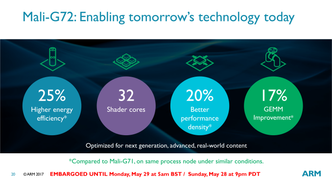
That said, the devil is in the details. And the details on Mali-G72 are all about optimizing. While ARM hasn’t made any high-level changes, the company has made a number of smaller, low-level changes that add up to a more significant impact for elevating Mali-G72 over Mali-G71. As a result the company is promoting the newer GPU design as offering 25% greater energy efficiency and 20% better performance density than Mali-G71, leading to a 40% performance improvement. Area and power efficiency are of course the lifeblood for mobile GPUs, and while the high-performance designs like the Mali-G71/G72 aren’t designed to push the envelope on area efficiency quite as much – favoring high performance instead – SoC vendors are all for trimming precious mm to reduce costs.
ARM isn’t offering a great deal of information on where all of these optimizations come from – it’s very much the sum of a large number of small changes – but at have provided us some key pieces of information. In particular, ARM has actually removed some complex instructions from their architecture, instead executing them over multiple clocks as other, simpler instructions. Excising instructions one big way to save on die space, allowing ARM to throw out the transistors that would be needed to execute those instructions. Obviously this is a double-edged sword – the emulated instructions are slower – but instructions that aren’t used very often likely aren’t worth the silicon. In this case I suspect we’d be looking at some especially esoteric things, such as atomic floating points.
ARM has also been doing some tinkering under the hood to improve the throughput of other desirable complex operations. This includes things such as the reciprocal square root and other reciprocal functions, which can now complete faster, but only for graphics (an interesting distinction, since the IEEE 754-compliant operation for compute remains unchanged). This goes hand-in-hand with a more broad set of tweaks to the internal datapaths for the ALUs, though besides further optimizing how data moves between the FMA and ADD/SF units, ARM hasn’t said much more.
However when it comes to overall performance efficiency, the big changes on Mali-G72 aren’t at the instruction level, but rather the cache level. All-told, ARM has tweaked buffers and caches at pretty much every step of the way. This includes making the L1 cache, the writeback cache, and the tiler buffer all larger. Meanwhile the instruction cache is unchanged in size, but ARM has tweaked the logic of it (presumably the algorithm used) to improve utilization by reducing misses.
All of this cache-related tweaks are geared towards the common goal of reducing memory bandwidth usage. Not only is this important for scaling performance with larger GPUs – GPUs get more powerful faster than memory bandwidth increases – but it improves power efficiency as well, as memory operations are relatively expensive. The overall performance improvement from the larger caches reducing misses certainly doesn’t hurt, either.
ARM in turn is particularly pitching the benefits of the cache changes for both graphics and machine learning tasks. In the case of graphics, their case study of choice found a 42% reduction in how much off-chip memory bandwidth was used in G-buffer writes, primarily due to the larger write buffer. Bear in mind this is likely a case of cherry-picking, but ARM isn’t off-base in that more complex scenes push the limits of smaller buffers (finally justifying the area cost of larger buffers). Meanwhile on the machine learning front, ARM is reporting a 13% improvement in SGEMM benchmark energy efficiency (and 17% for HGEMM thanks to the combination of cache changes and the earlier mentioned instruction changes. One of ARM’s big pushes for their entire lineup of SoC IP is for inference at the edge, so even small improvements help their standings overall.
Wrapping things up, we should see ARM’s new Mali-G72 design show up in devices in another year or so. While ARM isn’t responsible for the actual silicon their IP goes into – and as such, this is ultimately in the hands of SoC vendors – the Mali-G71 did show up on the HiSilicon Kirin 960 only about 8 months after its launch. So if a partner wants to push it, they could do Mali-G72 in a similar amount of time. Though something closer to Samsung’s roughly 1 year cadence is likely to be more par for the course.


