Samsung Foundry Update: 2nm Unveil in June, Second-Gen SF3 3nm Hits Production This Year
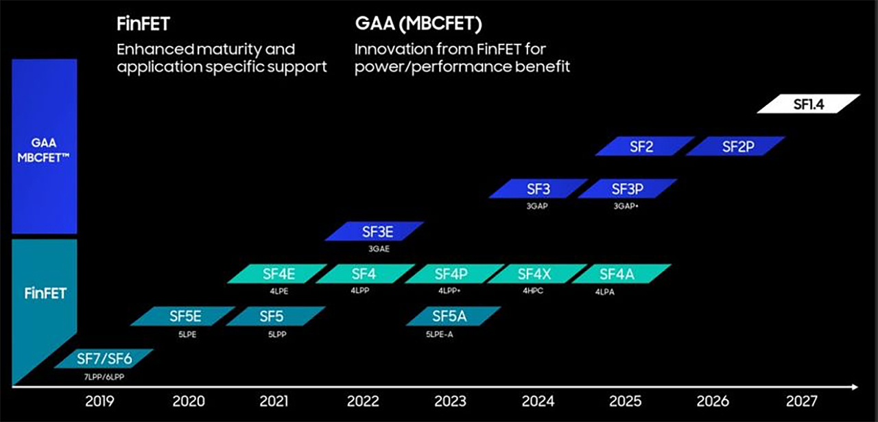
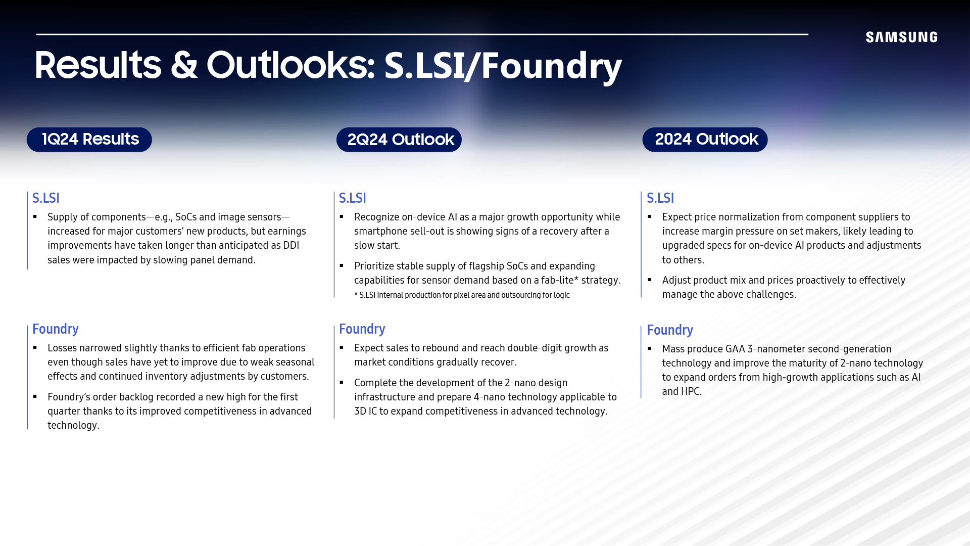
As part of Samsung’s Q1 earnings announcement, the company has outlined some of its foundry unit’s key plans for the rest of the year. The company has confirmed that it remains on track to meeting its goal of starting mass production of chips on its SF3 (3 nm-class, 2nd Generation) technology in the second half of the year. Meanwhile in June, Samsung Foundry will formally unveil its SF2 (2 nm-class) process technology, which will offer a mix of performance and efficiency enhancements. Finally, the company the company is preparing a variation of its 4 nm-class technology for integration into stacked 3D designs.
SF2 To Be Unveiled In June
Samsung plans to disclose key details about its SF2 fabrication technology at the VLSI Symposium 2024 on June 19. This will be the company’s second major process node based upon gate-all-around (GAA) multi-bridge channel field-effect transistors (MBCFET). Improving over its predecessor, SF2 will feature a ‘unique epitaxial and integration process,’ which will give the process node higher performance and lower leakage than traditional FinFET-based nodes (though Samsung isn’t disclosing the specific node they’re comparing it to).
Samsung says that SF2 increases performance of narrow transistors by 29% for N-type and 46% for P-type, and wide transistors by 11% and 23% respectively. Moreover, it reduces transistor global variation by 26% compared to FinFET technology, and cuts product leakage by approximately 50%. This process also sets the stage for future advancements in technology through enhanced design technology co-optimization (DTCO) collaboration with its customers.
One thing that Samsung has not mentioned in context of SF2 is backside power delivery, so at least for the moment, there is no indication that Samsung will be adopting this next-gen power routing feature for SF2.
Samsung says that the design infrastructure for SF2 – the PDK, EDA tools, and licensed IP – will be finalized in the second quarter of 2024. Once this happens, Samsung’s chip development partners will be able to begin designing products for this production node. Meanwhile, Samsung is already working with Arm to co-optimize Arm’s Cortex cores for the SF2 process.
SF3: On Track for 2H 2024
As the first fab to introduce a GAAFET-based node, Samsung has been on the cutting edge of chip construction. At the same time, however, that has also meant that they’re the first fab to encounter and solve the inevitable teething issues that come with such a major transistor design change. Consequently, while Samsung’s first-generation SF3E process technology has been in production for a little less than two years now, the only publicly-disclosed chips made on the process so far have been relatively small cryptocurrency mining chips – exactly the kind of pipecleaner parts that do well on a new process node.
But with that experience in hand, Samsung is preparing to move on to making bigger and better chips with GAAFETs. As part of their earnings announcements, the company has confirmed that their updated SF3 node, which was introduced last year, remains on schedule to enter production in the second half of 2024.
A more mature product from the get-go, SF3 is being prepared to be used for building larger processors, including datacenter products. Compared to its direct predecessor, SF4, SF3 promises a 22% performance boost at the same power and transistor count, or a 34% lower power at the same frequency and complexity, as well as a 21% logic area reduction. In general, Samsung pins a lot of hopes on this technology, as it’s this generation of their 3nm-class technology that is poised to compete against TSMC’s N3B and N3E nodes.
SF4: Ready for 3D Stacking
Finally, Samsung is also preparing a variant of their final FinFET technology node, SF4, for use in 3D chiplet stacking. As transistor density improvements have continued to slow, 3D chip stacking has emerged as a way to keep boosting overall chip performance, especially with modern, multi-tile processor designs.
Details on this node are limited, but it would seem that Samsung is making some changes to account/optimize for using SF4-fabbed chiplets in a 3D-stacked design, where chips need to be able to communicate both up and down. According to the company’s Q1 financial report, Samsung expects to complete their preparatory work on the chip-stacking SF4 variant during the current quarter (Q2).
Source: Recent News


