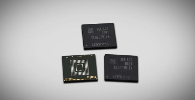
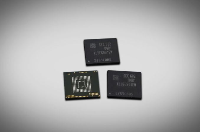
Samsung Announces 256GB UFS Embedded Storage Solution
Interestingly enough, we’re seeing something of a division in the mobile storage space, as it seems that some OEMs are focusing their efforts on UFS for internal storage, while others are moving towards NVMe over mobile PCI-E. Samsung Electronics seems to be staying with UFS for now, and recently announced their next generation of UFS 2.0 embedded storage solutions, which use 3D V-NAND to enable better NAND storage characteristics and to bump up the capacity from 128GB to 256GB.
By moving to V-NAND, random reads and writes are now at 45k and 40k IOPS, or 176 and 156 MB/s with 4KB blocks, which is well over double what shipped in the Galaxy S6. For sequential reads, speeds top out as high as 850 MB/s which is even faster than the 520 MB/s maximum of some SATA SSDs. Given that this is likely to be Samsung’s 30nm V-NAND process, I suspect that the storage density needed to achieve this kind of performance involves some sort of SLC/TLC hybrid, but in the absence of more information it’s hard to say.
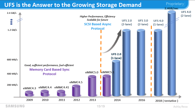
While the new NAND definitely is part of the speed improvement, it couldn't have been achieved without an increase of the interface bandwidth. The new memory today is the first announced UFS 2.0 solution based on a 2-lane interface. The UFS 2.0 standard defines a lane running at up to HS Gear 3 at up to 600MB/s, so doubling up of the lanes gives a theoretical maximum of 1.2GB/s. It’ll definitely be interesting to see what devices adopt this storage solution in the near future.


